-
E-mail
infochina@biolinscientific.com
-
Phone
18612271669
-
Address
Room 1205, Building 1, Zhanxiang Plaza, Lane 2290, Zuchongzhi Road, Pudong New Area, Shanghai
About Us
Sweden Biolink Technology Co., Ltd
Date: 2025-04-11Read: 0
The electronics industry can provide circuit boards and electronic components. The integrated circuits used in electronic devices are built on wafers made of semiconductor materials. Silicon is a widely used semiconductor material. Silicon wafers undergo rigorous cleaning procedures before chip manufacturing. Use a contact angle meter to measure the cleanliness of the surface of silicon chips. Polymers are also used in the electronics industry as insulation layer materials for chips and chip carriers, and the quality and uniformity of coatings are the most important.
[Surface Cleanliness - Cleanliness]
Do you need to characterize or evaluate surface cleanliness?
The surface surrounds us, everywhere. We live on it, utilize it, and make use of it. In many cases, surface cleanliness is of interest and importance, and in some cases even critical. The meaning of "cleanliness" is certainly a matter of definition, covering cleanliness at all scales from macro to nanoscale and beyond.
When we think of cleaning, the first type of surface that comes to our mind is the surface of the houses and objects we use in our daily lives - the kitchen, bathroom, clothes, and perhaps our transportation, such as our cars. But we also expect public places to be hygienic - restaurants, public transportation, and hospitals. The latter is one of the key areas where nanoscale cleanliness is crucial. For example, cleaning surgical tools and other surfaces in hospitals is key to successful surgery and preventing disease transmission. In industries farther away from us, such as the production and processing of food, pharmaceuticals, or other sensitive substances, shifting from manufacturing one component to another may require surface hygiene treatment between the two. Or in the electronics and optics industry, as well as in the manufacturing of circuits or coatings, the slightest dust molecule can be catastrophic. Other structures such as oil pipelines and heat exchangers in power plants may be exposed to pollution over time, accompanied by the accumulation of unwanted substances such as sediment formation, scaling, biofilm formation, and fouling, all of which may hinder their functionality.
Real time characterization and evaluation of surface cleanliness
QSense QCM-D can measure and quantify sediment, scale accumulation, and biofilm formation at the nanoscale, as well as remove the same sediment in real-time and quantitatively. Optimizing conditions to reduce or prevent the accumulation of unwanted substances is crucial, and you can characterize cleanliness before, after, and during environmental changes. In areas such as assessing kitchen cleanliness, describing biofilm formation, and measuring asphaltene adsorption in crude oil pipeline fouling, methods or additives can be developed to eliminate them.
Rapid evaluation of surface cleanliness through contact angle measurement
The efficiency of cleaning and detergent formulations can be evaluated through contact angle measurement.
The surface free energy of cleaning and treating surfaces is directly related to cleanliness and surface composition. Contact angle is one of the most sensitive surface analysis techniques, as even the nanoscale of the surface can affect wetting behavior. As a simple and fast measurement technique, contact angle is commonly used to track the efficiency of cleaning processes and cleaning solutions. Therefore, in the crucial field of cleanliness control, contact angle measurement is a very suitable quality control method. Automated Theta provides a user independent and fast method for contact angle measurement in cleanliness assessment.
The cleanliness of silicon wafers and circuit boards is an important factor in ensuring optimized functionality of the final product. The cleanliness of glass surfaces, such as inkjet printing of bottles or the use of adhesives for label applications, directly affects the quality of subsequent processing steps. Measuring glass contamination helps reduce waste and ensure efficient production.

ASTM C813-90- Hydrophobic Contamination of Glass by Contact Angle Measurement
[Surface Treatment and Coatings - Functional Nano and Nanoparticle Coatings]
Traditional coatings are typically used to protect the underlying materials or improve their visual appearance. In addition, coatings used for other functions have attracted increasing research interest. These types of coatings are commonly referred to as functional coatings.
Different functional coatings have a wide range of applications, but the most researched ones are anti fouling, antibacterial, conductive, self-cleaning, photochromic, self-healing, and superhydrophobic coatings.
Different coating strategies need to be adopted based on the functions that the coating needs to meet. Simple functional coatings can be prepared by using immersion coating, with minimal control over the structure and layer thickness of the coating. For more advanced coatings, Langmuir Blodgett and Langmuir Schaefer techniques can precisely control film thickness and encapsulation density. Langmuir Blodgett technology has been used for the deposition of nanoparticles for smart windows and graphene for electronic applications. QSense QCM-D can also be used to characterize the deposition of nanoparticles and the construction of functional nanocomposite structures.
There are several tools available for visual, molecular, and wetting characterization of coatings.
Characterization of superhydrophobic coatings
Superhydrophobic coatings have received widespread attention due to their applications on surfaces such as self-cleaning windows or anti icing surfaces. According to the definition, superhydrophobicity can be achieved when the static contact angle with water exceeds 150 ° and the contact angle hysteresis is low. Therefore, the characterization of superhydrophobic coatings can be achieved by measuring static and dynamic contact angles.
Watch the recorded webinar: Superhydrophobic surfaces - from laboratory to real-life applications
Blog post: Durability of superhydrophobic surfaces - the biggest obstacle to real-life applications
Deposition of nanoparticles for smart window coating
As we become increasingly concerned about the future of the Earth, different energy-saving methods are being studied more. Most of our energy consumption is used for heating or cooling buildings. There can be different solutions to improve the insulation performance of our buildings, and innovative smart windows have become a focus of attention. One interesting type of smart window is made of thermochromic materials, which can change color with changes in temperature. Therefore, windows coated with thermochromic films can control the heat exchange through the glass. In cold weather, store heat indoors; During hot weather, windows can prevent infrared radiation from the sun from entering buildings.
Researchers at University College London (UCL) have developed a method of coating glass surfaces with polystyrene nanospheres using Langmuir Blodgett (LB) technology [1]. They prepared highly ordered nanoparticle layers using LB, which can be used as etching masks in subsequent processes. The generated nanostructures can be coated with vanadium dioxide, giving the window the same anti reflective properties found in moth eyes. It reduces the amount of light reflected inside the room to less than 5%, which is much better than the effect obtained by other prototypes of vanadium dioxide coated windows [2].

Langmuir Blodgett technique was used to deposit 200nm diameter polystyrene nanospheres monolayers on a quartz substrate in a KSV NIMA medium-sized tank.
(a) The AFM image of a single molecular layer, (b) Fourier transform of the same image, demonstrates excellent crystallinity achievable using this technique. Copyright Dr. Alaric Taylor.
In addition to improving the reflective properties of windows, nanostructures can also self clean. The surface of the window is very water-resistant, which means that when raindrops fall on the surface, they form spherical droplets that easily roll off the window, collecting dirt, dust, and other pollutants and carrying them away. Especially for windows used in skyscrapers where window cleaning is challenging, this is a highly desirable performance. Researchers have extensively studied the self-cleaning performance of surfaces by using static and dynamic contact angle measurements.
[1] Taylor, A. Motheye smart windows Bio-inspired, temperature-responsive glazing for passive regulation of building temperature with the ability to self-clean (Unpublished doctoral thesis). (2016) University College London, London, UK.
[2] Taylor, A. et. al., A Bioinspired solution for spectrally selective thermochromic VO2 coated intelligent glazing, Optics Express 21 (2013) A752.
[Watch the recorded webinar: Deposition of Highly Ordered Nanoparticle Thin Films Using Langmuir Blodgett, Alaric Taylor, EPSRC Researcher at UCL University]
Blog Article: Highly Ordered Nanoparticle Thin Films
Deposition and characterization of graphene monolayers for electronic applications
Single layer graphene (SG) is the first truly two-dimensional material that has been proven to possess many excellent material properties, such as high conductivity and thermal conductivity, as well as high tensile strength. Many people believe that graphene is one of the most promising and multifunctional materials discovered so far. For example, the potential applications of this material include building smaller and faster electronic circuits, developing more powerful and flexible building materials, and creating more efficient batteries. Graphene can be used as both an n-type conductor and a p-type conductor. And due to its semiconductor properties, it has sparked speculation that it will one day replace silicon in electronic devices. One of the most interesting applications of single-layer graphene, due to its electrical properties, transparency, and good chemical resistance, is to replace indium tin oxide (ITO) or fluorine tin oxide (FTO) as solar cells and light-emitting diodes in optoelectronics. [1-3]
There are several different methods for preparing single-layer graphene. The most promising methods for large-scale industrial applications are different liquid-phase exfoliation methods, which typically generate dispersions of single-layer graphene or single-layer graphene oxide (SGO). The challenge is how to transfer single-layer graphene or single-layer graphene oxide from the dispersion to the support in a controlled manner. Langmuir Blodgett and Langmuir Schaefer (LS) deposition have recently shown promising results in the preparation of highly controllable graphene layers.
Characterization of graphene oxide films directly on Langmuir channels using Brewster angle microscopy and PM-IRRAS. PM-IRRAS can also be used to characterize thin films deposited on solid substrates.
Application Summary: Deposition and Characterization of Single Layer Graphene and Graphene Oxide Thin Films
Application Summary: Thin Film Structure Imaging: Brewster Angle Microscope
Application Overview: Manufacturing Highly Ordered Nanoparticle Thin Films
Functional coatings on the surface of solar panels
Solar cells (also known as photovoltaic cells) are electronic devices that directly convert light energy into electrical energy through the photovoltaic effect (see Figure 1). There are several types of available solar cells, the most common of which are manufactured on silicon wafers. Other types of solar cells include thin-film, dye-sensitized, and organic/polymer solar cells. Due to its simple manufacturing process, silicon solar cells are currently the most commonly used solar cells, holding over 80% of the market share, while other types of solar cells offer certain additional advantages such as flexibility.
At present, there are many active research groups in the field of photovoltaics in universities and research institutions around the world. This study can be roughly divided into three aspects:
·Make current technology solar cells cheaper and/or more efficient to compete with other energy sources.
·Develop new technologies based on the architecture design of new solar cells.
·Develop new materials as light absorbers and charge carriers.
The top layer of traditional solar cells is a thin protective glass coated with anti reflective (AR) coating. Anti reflective coatings are used to increase photon absorption and improve the efficiency of solar cells in this way. Sol gel dip coating technology is widely used to produce anti reflective coatings in large areas.
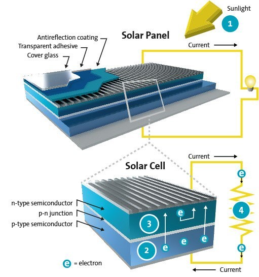
Ensuring good adhesion between different layers on solar cells is crucial during the manufacturing process. Contact angle measurement is usually used because good wetting indicates good adhesion.
Application Overview: Manufacturing Highly Ordered Nanoparticle Thin Films
Application Summary: Contact Angle Measurement in the Solar Cell Industry
Deposition of highly controllable nanofilms using Langmuir Blodgett method
[Functional Coatings - Sensors]
Living in today's society, information and predictability are highly valued, and we revolve around a large number of sensors to detect, detect, and measure various aspects of the surrounding environment. The amount of information collected every day is very large, with temperature, air pressure, light intensity, or toxic substances being just some examples.
Sometimes the collected data only provides us with information and convenience in daily life, such as giving us information so that we can decide whether to bring an extra sweater when going out. But it can also be used to determine whether adjustment and control are needed, such as verifying whether the pressure value remains within the preset maximum and minimum values. Each type of sensor is based on a specific detection method and can monitor parameters of interest.
Biosensors are a subclass of sensors. Biosensors utilize natural designed biometric systems for detection, such as target substances that bind to receptors. Then this information is converted and readings are collected. Sensors based on conductive polymers are being extensively studied due to their high potential applications. Langmuir Blodgett technology is capable of producing highly assembled controllable thickness films and has therefore been used in sensor applications,. These sensors have been used for gas sensors and detection of trace antibiotics in solutions. Different detection methods, from optical detection to conductivity measurement, are being applied.
QSense QCM-D as an Acoustic Biosensor
Biosensors are applied in many fields, such as medical applications, food industry, and national defense. In addition to biometric components, biosensors also consist of two parts: sensors that can detect biometric recognition and interpretable signal readout. Sensors can be based on different principles. A common sensor principle is acoustic sensing, such as quartz crystal microbalance (QCM). QCM technology based on piezoelectric principle for detection is a method in biosensing and has been used for decades in the development and application of biosensors.
As detailed in this widely circulated and detailed review of acoustic biosensors, the biological detection system of biosensors can be based on antibodies, proteins DNA、 Design and construct related modules for cells, lipid structures, carbohydrates, and nanoparticles. The scope of building modules and recognition components ranges from small to large, capable of detecting everything from heavy metal ions and DNA hybridization to cell attachment, proliferation, and growth, as well as cell response to external stimuli. The potential detection system has a wide range and is constantly exploring sensor interface processing strategies to improve its sensitivity and selectivity.
Conductive polymer based sensor
With the increasing emphasis on miniaturized devices, newly developed nanomaterials can further develop this field. Many of these materials cannot be prepared using traditional microfabrication methods, but instead utilize emerging technologies.
Conductive polymers such as polyaniline, polythiophene, polypyrrole, and their derivatives have been used as active layers for gas sensors and in the fabrication of immobilized enzyme biosensors. Sensors made of conductive polymers have many excellent characteristics, such as high sensitivity and short response time. Conductive polymers are also easy to synthesize and have good mechanical properties. The LB film analyzer can be used to prepare large-area highly controllable conductive polymer films.