-
E-mail
dawei.wang@germanlitho.com
-
Phone
18612023280
-
Address
Building 6, Qingdao Future Science and Technology Industrial Park, No. 106 Xiangyang Road, Chengyang District, Qingdao City
Qingdao Tianren Micro Nano Technology Co., Ltd
Micro lens array processing creates a micro optical "precision matrix"
Date: 2025-07-17Read: 1
In cutting-edge fields such as optoelectronics, imaging technology, and artificial intelligence,Micro lens array processing technologyStrict requirements, related to performance and application expansion, the following will analyze the key points from multiple aspects.
Material selection is the foundation, which needs to take into account both optical properties and mechanical stability. Quartz, with its ultra-high transmittance and low refractive index temperature coefficient, is an ideal choice in the ultraviolet to near-infrared wavelength range. It can accurately focus light and reduce chromatic aberration interference; Polymethyl methacrylate (PMMA) is suitable for infrared imaging and lightweight demand scenarios due to its good plasticity, lightweight, and moderate refractive index, making it conducive to large-scale preparation. After selecting the material, strictly control the purity, as even trace impurities may scatter light and reduce the uniformity of the array.
Precision control runs through the entire machining process, with dimensional tolerances almost as precise as a millimeter. The diameter deviation of a single micro lens needs to be controlled at the sub micron level to ensure tight array arrangement and uniform spacing, otherwise the optical path will be disrupted, imaging distortion or coupling efficiency will drop sharply; The surface roughness also requires a nanometer level, and a smooth surface ensures that light refraction and reflection follow the design trajectory, reducing scattering losses. This poses a high challenge to the resolution and process stability of processing equipment.
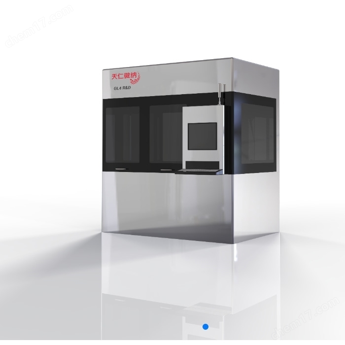
The process steps are interrelated, and photolithography technology uses deep ultraviolet lithography to accurately transfer the design pattern to the substrate, with a resolution of less than 100 nanometers, outlining the outline of the micro lens prototype; Continuing with the etching process, dry etching has excellent anisotropy and can vertically etch materials, ensuring steep sidewalls of the lens. Wet etching relies on selective etching with chemical solutions to soften edges or adjust curvature, and the two work together to create an ideal curved surface shape. Hot melt molding is also crucial, precisely controlling temperature and time to allow the material to flow and reshape in a solid state, correcting curvature errors, and shaping high-precision optical surfaces.
The atomic force microscope lightly scans the detection process, drawing a three-dimensional surface contour and quantifying roughness and curvature radius; The optical detection system simulates the actual optical path, projects parallel light, analyzes focusing and diffraction effects, and provides real-time feedback on processing defects for timely rework. From material selection to meticulous craftsmanship, and then to rigorous testing, the processing of micro lens arrays is carried out step by step, empowering technology to move towards higher performance dimensions.