-
E-mail
lu.yan@leboscience.cn
-
Phone
13584134215
-
Address
5th Floor South, Building A, Chuangzhi Industrial Park, 201 Jinshan Road, Jiangyin, Jiangsu
Jiangsu Leibo Scientific Instrument Co., Ltd
The working principle and application fields of magnetron sputtering coating equipment
Date: 2025-12-18Read: 2
1、 Overview and Industry Background
1.1 The Position of Magnetron Sputtering
Magnetron sputtering isPhysical Vapor Deposition (PVD)One of the commonly used and efficient methods for thin film preparation in technology. It utilizes a magnetic field to confine electrons in the plasma, increasing gas ionization rate, thereby achieving high-speed and uniform thin film deposition at lower pressures and substrate temperatures.
withSemiconductors, display panels, new energy, surface engineeringThe requirements for thin film performance (thickness uniformity, controllable composition, adhesion, density) in various fields are constantly increasing, and magnetron sputtering equipment has become a core manufacturing equipment.
1.2 Industry Development Trends
Advanced semiconductor processesMetal interconnect layers, barrier layers, dielectric layers, etc. require high uniformity and purity of thin films.
Display and OptoelectronicsLarge scale production of ITO transparent conductive film, metal gate, and optical multilayer film.
new energyThin film solar cells (CIGS, CdTe), lithium battery electrodes, and solid electrolyte coatings.
Functional coatingHard alloy cutting tools, wear-resistant layers for molds, decorative coatings.
The global market for magnetron sputtering equipment has grown steadily, especially in Chinese Mainland, Taiwan, China, South Korea and Japan, which are active in capacity expansion and technology iteration.
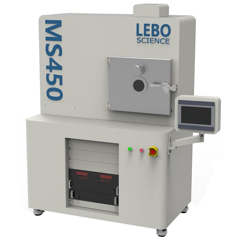
2、 Working principle
2.1 Basic Physical Processes
The core of magnetron sputtering is to utilizeHigh energy ion bombardment on the surface of the target material, causing atoms or molecules of the target material to escape (sputtering) and deposit a thin film on the surface of the substrate. The main steps are as follows:
Establishment of vacuum environment
Extract the chamber to a high vacuum (10 ⁻⁴~10 ⁻⁶ Pa) to reduce residual gas contamination of the film.
Fill in working gas
Generally, it is argon gas (Ar), and some processes add reaction gases (O ₂, N ₂, CH ₄, etc.) to form compound thin films.
Plasma generation
Applying high voltage (DC or RF) between the target material and the substrate triggers glow discharge, forming a plasma containing Ar ⁺, electrons, etc.
Magnetic field constrains secondary electrons
Arrange permanent magnets or electromagnetic coils near the surface of the target material to form a closed magnetic field (commonly known as a "track shaped" magnetic field), which causes secondary electrons to spiral along magnetic field lines, extending their path in the plasma region, significantly improving the ionization rate of argon gas, enhancing sputtering efficiency, and reducing substrate temperature rise.
Atomic sputtering of target material
High energy Ar ⁺ bombards the target material, and the target atoms gain kinetic energy to detach from the lattice and fly towards the substrate.
thin film deposition
Sputtering atoms migrate, nucleate, and grow into thin films on the substrate surface; If a reactive gas is introduced, it can react on the surface to form compound films such as oxides and nitrides.
2.2 Magnetic Field Effect and Advantages
Improve ionization rateExtended electron path → More Ar atom ionization → Higher sputtering yield
Reduce substrate temperatureReduce direct bombardment of high-energy electrons on the substrate → Low thermal load, suitable for heat sensitive substrates
Increase sedimentation rateCompared to ordinary diodes, the sputtering rate can be increased several times
Improve the uniformity of film thickness: Plasma density distribution is more uniform → good consistency in large-area deposition
3、 Main types
4、 Application fields in thin film deposition
4.1 Semiconductors and Microelectronics
Metal interconnect layerMetal thin films such as Cu, Al, and W are used to fill the internal wires and contact holes of chips.
Barrier layer/seed layerTi, TiN, Ta, TaN prevent metal diffusion and promote the adhesion of electroplating seed layers.
Dielectric layerSiO ₂ and Si ∝ N ₄ are used as insulation and passivation layers.
4.2 Flat Panel Display and Optoelectronics
Transparent Conductive Film (TCO)ITO (In ₂ O ∝: Sn) and AZO (ZnO: Al) are used for LCD/OLED electrodes and touch screens.
Metal gate and reflective layerAg, Al, Mo are used for backplate metal circuits and reflection enhancement.
optical thin filmMultilayer dielectric films achieve functions such as anti reflection, high reflectivity, and filtering.
4.3 New Energy Sector
Thin film solar cellsCIGS and CdTe absorption layers; ZnO and i-ZnO window layers.
lithium batterySilicon based and carbon based negative electrode coatings; Solid electrolyte thin film.
fuel cell:Pt、 Deposition of carbon supported catalyst thin film.
4.4 Surface Engineering and Functional Coatings
Hard coatingTiN, CrN, TiCN improve the wear resistance of cutting tools and molds.
Anti corrosion/decorative film:Ni、Cr、Au、 Colored TiO ₂ is used for hardware, clocks, and architectural decoration.
Thermal barrier coating (in combination with other processes)YSZ (Yttrium Oxide Stabilized Zirconia) and other ceramic films.
5、 Technological advantages and challenges
5.1 Advantages
Controllable composition: Can prepare pure metal, alloy, and compound thin films
Strong adhesion of film layerHigh energy particle bombardment enhances interface bonding
Good uniformity over a large areaSuitable for industrial continuous production
Good process repeatability and easy automation
5.2 Challenge
Low utilization rate of target materialCircular target material has fast center sputtering and slow edges, with a utilization rate typically less than 30%; Can be improved to a rotating target.
Uneven plasmaLarge scale sedimentation is prone to thickness/composition gradients, requiring optimization of magnetic field and airflow design.
High difficulty in controlling reactive sputteringThe partial pressure of the reaction gas needs to be precisely controlled, otherwise target poisoning (arc discharge caused by insulation compound coating the target surface) may occur.
High equipment investment and maintenance costsThe vacuum system, power supply, and magnetic field system are precise and require high maintenance technology.
6、 Development Trends
High power pulsed magnetron sputtering (HiPIMS)High peak power generates high ionization rate plasma, which can prepare nanocrystalline or columnar thin films with more block like properties, improving the density and performance of the film layer.
Large area/roll to roll (R2R) sputteringTargeting flexible displays and thin-film photovoltaics, achieving continuous production and reducing costs.
Intelligence and digital controlIntroducing PLC+MES system to achieve real-time monitoring and adaptive adjustment of process parameters, improving yield and consistency.
Green ManufacturingReduce harmful gas emissions, improve the utilization rate of target materials, and develop recyclable target material technology.
Multi functional composite sedimentationCombining ion beam assistance and plasma pretreatment to achieve interface modification or integrated deposition of multi-layer heterostructures.
7、 Conclusion
Magnetron sputtering coating equipmentby virtue ofHigh speed, uniform, and controllableThe ability to deposit thin films has played an important role in fields such as semiconductors, optoelectronics, energy, and surface engineering. With the advancement of high-power pulses, large-area continuity, and intelligent control, it will play a greater role in the next generation of high-performance thin film manufacturing. Industry participants need toTarget material optimization, plasma uniformity control, equipment intelligenceContinuously innovate in various aspects to meet the growing demand for high-quality films in the market.