-
E-mail
qeservice@enli.com.tw
-
Phone
18512186724
-
Address
Room 409, Building A, No. 169 Shengxia Road, Pudong New Area, Shanghai
About Us
Guangyan Technology Co., Ltd
Date: 2025-07-14Read: 1
Research difficulties and challenges

Existing efficient charge selective contact layers, such as self-assembled monolayers,SAMs)Optimization is mainly focused on narrow bandgap perovskite solar cells, but their energy level characteristics are not comparable to wide bandgap ones(WBG)Tailored design for perovskite. This interface energy level mismatch leads to severe non radiative recombination, directly causing open circuit voltage loss and reduced fill factor, severely limiting the overall power conversion efficiency of the device.
The core challenge of this study lies in how to systematically andAccurately regulateSAMEnergy levelMake it compatible withWBGCalcium titanium ore layer reachesbest matchThusReduce interface recombination loss and improve charge extraction efficiency, improveWBGThe overall performance of perovskite sub cells and stacked cells.
Research Team and Publication
This groundbreaking study was conducted byProfessor Xue Jingjing from Zhejiang University andDeren Yang教授Co leadership, research results published in internationally renowned academic journals Nature CommunicationsThe team demonstrated how to utilize the molecular structureInduced effectAccurately and systematically regulateSAMsAnd based on this, high efficiency was preparedWBGPerovskite single junction battery andRecord breaking efficiency of perovskite/TOPConstacked battery.
Research achievements and highlights
l Core innovation: Successfully utilizing the "induction effect" in molecular structure(Inductive Effect)To precisely and systematically regulate self-assembled monolayers(SAMs)The energy level.
l implementSAMsEnergy level optimization to match wide bandgap(WBG)The demand for perovskite batteriesSolved the efficiency bottleneck caused by energy level mismatch.
l Confirm the presence of strong electron donating groupsPyAA-MeO SAMsConstructed the most favorable interface energy level alignmentSignificantly promoted hole extraction and significantly reduced non radiative recombination losses.
l Prepare high-performanceWBGPerovskite single junction battery, power conversion efficiency(PCE)Highest achieved22.8%And has a high open circuit voltage(VOC)And fill factor(FF).
l The device exhibits excellent stabilityIt performs well in various accelerated aging tests such as lighting, thermal stress, and maximum power point tracking.
l Based on optimizedSAMsSuccessfully constructed high-performance perovskite/TOPConStacked batteries have achieved31.1%Power conversion efficiency(Third party authentication is30.9%).
l Through analysisPLQYAs a result, extraction and quantification were carried outQuasi Fermi level splitting(QFLS)The gain,PyAA-MeOmix intoThe perovskite thin film exhibitsthe largestQFLSgain(48.1 meV)Compared to the highest observed in photovoltaic devicesVOCThe performance matches,Reflecting the reduction of non radiative recombination losses.
l The efficiency of this stacked battery is currently reported for perovskite/TOPConOne of the high efficiencies in stacked batteries.
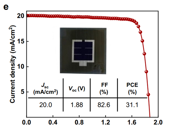
Fig 4e
Experimental process and steps
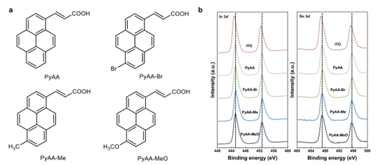
Figure1ab
Molecular Design and Synthesis The research team designed and synthesized a series of pyrene based core structures with acrylic anchoring groupsSAMMolecules, includingPyAAThePyAA-BrThePyAA-MeandPyAA-MeOEach molecule has different electronic properties and functional groups.
SAMsthin film preparation To synthesizeSAMMolecules dissolve in specific solvents and are coated using spin coating methodITODeposition forms a single-molecule thin film on the substrate, followed by annealing treatment to stabilize the film structure.
Preparation of Perovskite Thin Films InSAMsmodifiedITOOn the substrate, prepare a wide bandgap perovskite precursor solution, deposit perovskite thin films using spin coating and anti solvent treatment techniques, and perform annealing treatment.
Preparation of Single junction Solar Cells withSAMsmodifyITOAs the substrate, sequentially deposit perovskite layers, and then deposit electron transport layers through thermal evaporation method(LiFTheC60TheBCP)And silver electrodes are used to complete the inverted structure of single junction perovskite solar cells.
Preparation of stacked solar cells Optimizing wide bandgap perovskite sub cells (based onPyAA-MeO)Integrate into commercializationTOPConCrystalline silicon sub battery. InTOPConSequential deposition on silicon substrateNiOxLayerSAMsCalcium titanium layer, surface passivation layer, and intermediate layer(LiFTheC60TheSnO2)And the top electrode structure(INFORMATIONTheAgTheLiF)Assemble into perovskite/TOPConStacked solar cells.
Theoretical calculation assistance Using density functional theory and first principles computational simulationsSAMMolecules inITOThe surface structure and interactions assist in understanding experimental observation phenomena and guide experimental design.
characterizationsquareLaw and Results
1.J-VCharacteristic measurement
The research team uses simulationAM 1.5 Gspectrum(100 mW cm-2)Source measurement unit under illumination(Keithley 2400)conductJ-VCharacteristic measurement. Accurate and reliableJ-VMeasurement requires high-quality solar simulators,Guangyan TechnologyEnlitech SS-XSolar simulator, itsAM1.5GThe filter adopts advanced plasma deposition technology, which has high spectral accuracy and excellent durability.
The results show that based on different factorsSAMsThe wide energy gapPSCsIts average efficiency ranges fromPyAA-Brof12.9%Gradually increase toPyAA-MeOof22.1%Among them,PyAA-MeOThe device on the substrate performs the best and achieves22.8%ofPCE, possessing1.24 VofVOC、84.3%ofFFand21.8 mA cm-2 ofJSC.

image4aPresented based on differentSAMsofPSCsdeviceJ-VCurve,table1Summarized the performance parameters of these devices.

image4eIt shows the stacked batteryJ-VCurve.
2.External quantum efficiency(EQE)measurement
Measure the efficiency of generating charge carriers in batteries under different wavelengths of light and verify itJ-VIn measurementJSCValue. The research team usesEnlitech QE-RExternal quantum efficiency integration systemThe measurement was conducted under short-circuit conditions using a lock-in amplifier and a current preamplifier.EQEMeasurement can understand the response of batteries in different spectral ranges.Guangyan TechnologyEnlitech QE-RQuantum efficiency measurement system, with high repeatability(> 99.5%)Equipped with two independent two-phase lock-in amplifiers, it can simultaneously monitor optical power and device signals.

image4b Compared based onPyAAandPyAA-MeOThe device'sEQECurve.PyAA-MeOThe base deviceEQEThe curve shows a higher response, as calculated by integrationJSCvalue21.0 mA cm-2, higher thanPyAAThe base device20.2 mA cm-2.EQEThe increase in integrated current is attributed to the improved energy alignmentMore effective hole extraction.
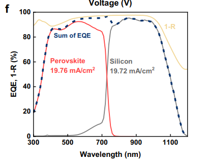
image4f Displays perovskite/In silicon stacked devicesWBGSub cells and silicon sub cellsEQECurve, integralJSCThe values are respectively19.8 mA cm-2 and19.7 mA cm-2.
3.Quasi Fermi level splitting(QFLS)Related optical characterization
QFLS (Quasi-Fermi Level Splitting)Described the non-equilibrium energy level distribution of photo generated carriers under illumination, used to quantify the properties of materialsVOCPotential and help understand the sources of non radiative composite losses. The research team measured based on differentSAMsThe perovskite thin filmPLQYThe research team usesEnlitech LQE-50-EL(LQ-50)Electroluminescence External Quantum Efficiency System, CollectEQEEL.
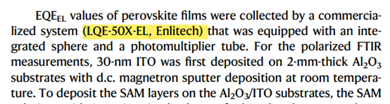

throughPLQYMeasurement and research have found that its value varies withSAMFunctional groups enhance their electron donating ability and increase, fromPyAA-Brof0.70%Rise toPyAA-MeOof5.71%Quasi Fermi energy splitting based on this calculation(QFLS)The enhancement value also shows the same trend, fromPyAA-Brof17.2 meVIncrease toPyAA-MeOof48.1 meV, PyAA-MeOShow the maximumQFLSenhanceThis is the highest open circuit voltage of its device(VOC)Highly consistent. In addition, the entire deviceEQEELFurther measurements have confirmed that,EQEELThe value increases with the enhanced electron donating ability of functional groups, makingPyAA-MeOVoltage loss of devices(ΔV)minimum(only0.18 mV)These excellent optoelectronic performance indicators are derived from favorable interface energy alignment,Promoted efficient hole extractionandSignificantly reduced interface charge recombination.

Guangyan Technology has launched a new productQFLS-MaperPredict material limits!
Enlitech QFLS-Maper,1/5The equipment price is sufficient for useMappingFunctional outputQFLS imageVisualizing the overall quasi Fermi level distribution, the quality of the material is clearly visible!
Follow us for more latest news!
4.Transient photocurrent(TPC)Attenuation measurement
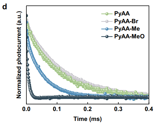
Study the extraction kinetics of charge carriers (holes) under short-circuit conditions. The optimization of interface energy alignment caused by the induction effect of electron methoxy groups effectively promotes the rapid extraction of holes.(image3d)
Other characterizations
1.XX-ray diffraction(XRD):Evaluate the crystalline quality of perovskite thin films. The peak positions and intensities of each sample are almost the same, and almost no observations are madePbI2 The Peak33This indicates that different functional groups have little effect on the crystallization of perovskite.(image2a)

2.Two dimensional grazing incidence wide-angleXRay scattering(2D GIWAXS)
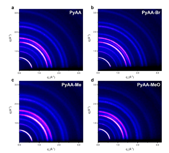
Study the crystal orientation of perovskite thin films deposited on different substrates. In all four cases, the crystal orientation of perovskite films is similar. This further confirms the changeSAMFunctional groups have no significant effect on the crystallization and orientation of perovskite films.(imageS 24)
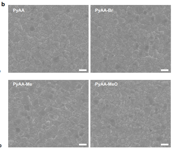
3.scanning electron microscope(SEM)
Observe the surface morphology of perovskite thin films.SAMThe modification of functional groups has a negligible impact on the quality of the perovskite layer film deposited above.(image2b)
4.ultraviolet-Visible spectrum(UV-vis spectroscopy)
Evaluate the optical absorption characteristics and bandgap of perovskite thin films. The similar spectral shapes and intensities indicate that changes in functional groups do not alter the light absorption and optical bandgap of perovskite materials.(image2c)

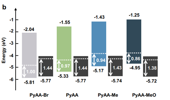
5.Ultraviolet photoelectron spectroscopy(UPS)
obtainSAMmodifiedITOSurface energy level information and analysisSAMAlign the energy with the perovskite interface. Prove that the observed improvement in energy alignment is mainly due toSAMChanges in energy levels.(image3b)
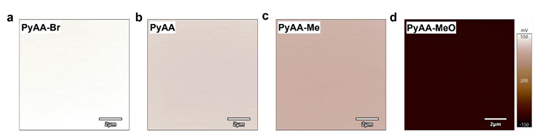
6.Kelvin probe force microscope(KPFM)
measurementSAMSurface potential changes of modified surfaces. The surface potential decreases as the electron donating ability of functional groups increases, indicating thatPyAA-BrtoPyAA-MeOofpType behavior is becoming increasingly apparent.(imageS 30)
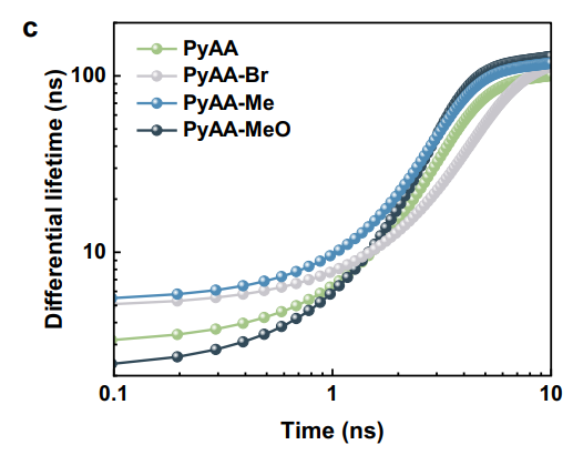
7.Time-resolved photoluminescence(TRPL)
Study the carrier dynamics in perovskite thin films, especially the charge extraction process.PyAA-MeOThe first interval in the differential lifetime curve of the base sample is the shortest, which is mainly dominated by the charge transfer process, confirming thatPyAA-MeOExcellent interface charge extraction capability.(image3c)
9.time-resolvedPLSpectrum andPL Mapping
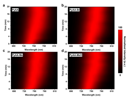
Evaluate the photostability of perovskite thin films. illumination 24 After hours, all samplesPLThe launches all showed similar redshifts. This confirmsSAMThe influence of functional groups on the phase stability of wide bandgap perovskite films can be ignored.(imageS 26.27)

10.Maximum power point tracking(MPPT)stability test(MPPT stability test)
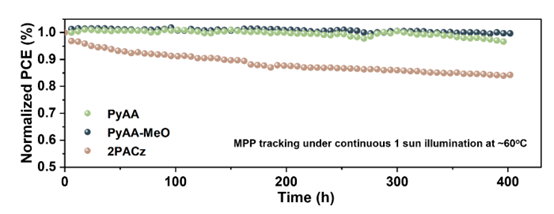
Evaluate the long-term stability of the device under continuous illumination.imageS 39 providedMPPTTrack the curve. Unpackaged devices in research reports60 °CNext up 400 hourMPPTAfter testing, based onPyAA-MeOThe device has retained more than99%The initial efficiency. at about 2500 In different accelerated aging tests of the hour, its efficiency still remains above96%, demonstrating its enhanced resistance to external stimuli.
11.Accelerated aging test(Accelerated aging tests)
Evaluate the long-term lifespan of the device under accelerated conditions. The device is around 2500 Can still retain more than hours later96%The initial efficiency.
Research Summary
precise regulationSAMsStrategy of energy level The research has successfully developed a strategy for precise and systematic regulation of self-assembled monolayer energy levels using functional group induced effects, providing a key method for customizing interfaces to match specific bandgap perovskites.
Optimize interface energy level and charge extraction By introducing methoxy groups with strong electron donating ability(PyAA-MeO)Successfully optimizedSAMAlign the interface energy levels with wide bandgap perovskite to create band bending favorable for hole extraction, as confirmed by experimentsPyAA-MeOHas excellent interface charge extraction ability.
Single settlementWBGThe High Efficiency of Perovskite Batteries Using energy level optimizationPyAA-MeOAs a hole selection layer, it significantly improvesWBGPerovskite solar cell performance, device achieves22.8%The photoelectric conversion efficiency is mainly attributed to improved interface hole extraction and reduced non radiative recombination losses.
Effectively reduce non radiative recombination and voltage loss Optimized interface energy level alignment and efficient hole extraction effectively reduce non radiative recombination of devices.PLQYTheQFLSTheEQE_ELTests have shown that,PyAA-MeOThe device has non radiative recombination loss and minimal open circuit voltage loss.
Realize high-efficiency stacked solar cells High performance will be achievedWBGPerovskite sub cells (usingPyAA-MeO)Integrate into commercial useTOPConCrystalline silicon sub cell successfully constructs high-performance perovskite/TOPConStacked solar cells.1 cm2Active area stacked devices achieve31.1%Efficiency (third-party certification)30.91%), forTOPConOne of the reported high efficiencies of stacked batteries.
Show device stabilityPyAA-MeOThe device exhibits excellent operation and thermal stability. Unpackaged devices undergo accelerated aging testing, including maximum power point tracking, continuous illumination, and continuous heating, and maintain their performance even after prolonged operation96%-99%The initial efficiency.
SAMsSlight impact on perovskite thin films Different functional groupsSAMsThe crystallization, morphology, optical properties, and photostability of the perovskite film deposited on it have little effect, further confirming that the improvement in device performance is mainly attributed toSAMImprovement of the interface with perovskite, rather than changes in the perovskite film itself.
Reference from Nature Communications_SOI: 10.1038/s41467-025-59896-8
This article is rewritten by Enlitech for scientific research and academic sharing. If there is any infringement, please inform us by email