-
E-mail
qeservice@enli.com.tw
-
Phone
18512186724
-
Address
Room 409, Building A, No. 169 Shengxia Road, Pudong New Area, Shanghai
About Us
Guangyan Technology Co., Ltd
Date: 2025-08-21Read: 1
Research background and challenges
PSCThe key bottleneck of commercialization lies in the insufficient reproducibility of defect passivation processes. This study addresses the three core challenges faced in this field:
1. Surface state variabilityThe surface state of perovskite thin films varies significantly among different batches and operators, and even small process fluctuations (temperature, stoichiometry, humidity) can lead to vastly different defect distributions, making it difficult to reproduce passivation effects.
2. Difficulty in controlling the optimal concentration of passivating agentTraditional strategies need to find a balance point (optimal concentration) between defect repair and charge transferC*)However, surface state variations result in the inability to reproduce established optimal conditions across experiments, and even have negative effects.
3. The inherent limitations of conventional passivation modes:CPThe concentration change of passivating agent in the mode significantly affects its distribution and energy level alignment, affecting reproducibility. Excessive passivating agents can easily form residual powders and low dimensional phases, leading to high interface resistance, decreased device performance, and initial stability issues.
Research Team and Solutionsmethod
This is about perovskite solar cells(PSCs)Research on Defect Passivation Strategy, byProfessor Wang Rui from Xihu University and Professor Xue Jingjing from Zhejiang UniversityCompleted by a team led jointly. Their research results have been published in top international journals Natural Energy(Nature Energy)Up there.
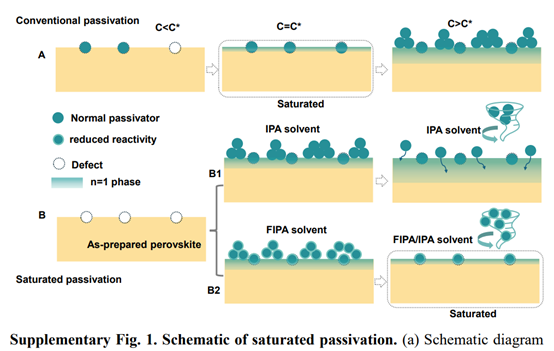
The research team proposed that 'Saturation passivation "(Saturated Passivation, SP)New strategyAdopting an innovative two-step approach to address the aforementioned challenges:
Step 1: Activity regulation
Use fluorinated isopropanol(FIPA)Reduce the reactivity and permeability of passivating agent molecules, allowing the use of high concentrations of passivating agents to ensure that all surface defects are fully passivated, while avoiding excessive reactions and the excessive formation of harmful low dimensional phases.
Step 2: Precise cleaning
adoptFIPAWith isopropanol(IPA)Rinse with mixed solvents to accurately remove excess non binding passivating agent molecules, achieve defect saturation passivation, and maintain the low dimensional layer at an appropriate thickness.
Key research achievements
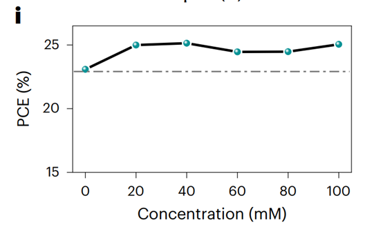
Fig. 3i
1. FIPAMechanism of solvents:FIPAStrong hydrogen bonding between fluorine atoms and ammonium passivators(H–FHydrogen bonding), competitive inhibitor passivator andPbI2The excessive reaction effectively reduces the reactivity and permeability of passivators, avoiding the excessive formation of harmful low dimensional phases.
2. Significantly expanding the operating window :SPThe strategy has a high tolerance for concentration deviations of passivators, compared to traditional methodsCPThe mode provides a wider range of appropriate concentrations, greatly improving process reproducibility.
3. device performance
Efficiency breakthrough:n–i–pLow bandgapPSCreach25.6%Thep–i–nLow bandgapPSCreach26%Thep–i–nwide bandgapPSCreach23%The1 cm2large areaPSCreach24.5%
Stability improvement:1000After accelerating aging for hours, it still remains above80%initialPCEThe initial stability is significantly better thanCPdevice
Reduced hysteresis phenomenonDefect passivation effectively inhibits ion migration
4. Extensive universality verification SPThe strategy is applicable to:
Different device structures(n–i–pThep–i–n)
Multiple perovskite compositions (different)BrContent)
Diversified preparation techniques (two-step method, anti solvent deposition method)
Different preparation environments (nitrogen, air)
Multiple device areas (more significant for large-area devices)
Can be achieved through immersion method, with industrial potential
Experimental steps and process
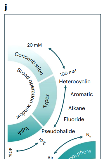
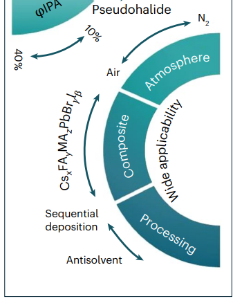
Fig. 4j
1. Preparation of Perovskite Thin Films Verification using two main sedimentation methodsSPStrategy universality:
two-step methodLayered spin coatingPbI2Solution andFAI/MAClAnnealing after solution, suitable forn-i-pandp-i-nLow bandgap and wide bandgap perovskite structures
Anti solvent deposition methodDuring the process of spin coating precursor solution, add anti solvent (such as anise ether or ethyl acetate) dropwise and turn off the heat
Preparation environment includes nitrogen glove box (high purity) and air environment(25-30%Humidity, simulating actual production conditions.
2. Device assembly
Substrate structure:ITOorFTODeposition of electrons on glass substrate/Hole transport layer(SnO2The2PACzTheNiOx/Me-4PACZEtc.)
SPpassivation treatmentHigh concentration ammonium salt passivator(PEAIDissolve inFIPASpin coating onto the surface of perovskite, followed byFIPA / IpanRinse with mixed solvents to remove excess molecules.p-i-nStructural components require brief low-temperature annealing
Alternative methodsVerify the feasibility of using immersion method instead of spin coating method
Electrode completedSedimentary hole transport material(Spiro-OMeTAD)Or electronic extraction layer(LiF/C60/BCP)Finally, evaporate the metal electrode
3. performance testing Measurement under standard conditionsJ-VCharacteristic curve, obtainedPCETheVOCTheJSCTheFFWaiting for key parameters. All measurements have not been preprocessed and are specifically targeted towards1 cm2Industrial potential assessment of large-area devices.
Characterization methods and results
Quasi Fermi level splitting(Quasi-Fermi Level Splitting, QFLS)
Evaluate the defect passivation effect and non radiative recombination loss suppression ability of perovskite thin films,QFLSEnhance directly associated devicesVOCandFFimprove.
sutra100 mM PEAI/FIPAProcessed perovskite thin filmQFLSfilmThe improvement is significant17.5 mVSignificantly better thanPEAI/IPAprocessed12.8 mVThe cleaning steps may vary depending onPEAIPowder dissolution or2DDegradation reduces the degree of improvement, butIPAcleanedQFLSfilmThe improvement is slightly higher thanFIPAwash.SPProcessed filmQFLSfilmContinuous improvement,PLNo significant changes were observed in the spectrum2DThe phase emission peak confirms the stable passivation effect.
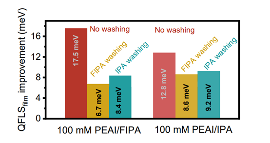
imageS 12 display100 mM PEAI/FIPAandPEAI/IPAProcessing thin films without cleaningFIPACleaningIPACleaning under three different conditionsQFLSfilmImprove comparison.PEAI/FIPAThe unwashed sample shows the highest improvement value(17.5 mV)Visually present the impact of different solvent treatment and cleaning steps on defect passivation effect.
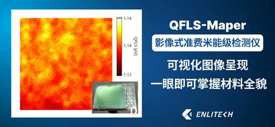
Latest Release from Guangyan TechnologyQFLS-MaperAnalyze the upper limit of material potential!
Enlitech QFLS-MaperLet you use toolscompetitiveness1/5cost advantageBy doing so, one can acquire the ability to map spatial distribution andQFLSimaging technologyClearly display the spatial distribution of quasi Fermi levels, making the quality of materials clear at a glance!
Track our updates and get information as soon as possible!
current density-voltage(J-V)curve
Characterize the core performance parameters of solar cells, reflecting device charge transfer and overall photovoltaic performance.
SPSignificant improvement in various strategiesPSCsofPCEPerformance.Cs0.05FA0.95PbI3 p-i-nStructural componentsPEAI-SPAfter processing,PCEreach, achieve, attain25.5%(VOC = 1.17 V,FF = 83.00%,JSC = 26.30 mA cm-2). This strategy applies to different components of perovskite(20% FAPbBr3or40% MAPbBr3Doping, different preparation methods, and different environments all demonstrate excellent universality.SPPassivation effectively reduces hysteresis phenomenon, attributed to defect passivation inhibiting ion migration.
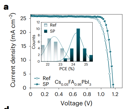
image4a Display reference devices andPEAI-SPprocessedCs0.05FA0.95PbI3 p-i-nstructural deviceJ-VCurve comparison andPCEStatistical histogram.SPThe processing device curve is more 'square', displayingHigher fill factor and power conversion efficiency,PCEMore concentrated distribution and higher average value, highlightingSPThe strategy has a significant effect on improving device performance and repeatability.
External quantum efficiency(External Quantum Efficiency, EQE)
The efficiency of converting incident photons into output current under different wavelengths of illumination directly reflects the spectral response capability of the device and the effectiveness of solar light utilization. Measurement is conducted usingEnliTech QE-RQuantum efficiency measurement system.
EQESpectral data supportJ-VMeasured by the curveJSCValue, further verify the performance of the device in various spectral regions, and confirmSPThe photoelectric conversion capability of the device after strategic processing.

imageS 22a displayCs0.05FA0.95PbI3 p-i-nstructural deviceEQESpectrum. The device operates in the visible and near-infrared regions (approximately300-850 nm)DisplayHigh quantum efficiency, peak value close to90%Confirm that the device has efficient light absorption and charge collection capabilities in this wavelength range.
Maximum power point tracking(MPP tracking)
Monitor the current output of the monitoring device over time under constant illumination and bias voltage, evaluate long-term operational stability, especially performance under accelerated aging conditions.
Under simulated accelerated aging test conditions(65°CTheN2In the glove box0.8Times the sunlight),SPStrategy demonstrates stability.SPDevices in1000After hour testing, it still retains more than80%initialPCEHowever, traditional passivation(CP)At the beginning, the device260Within hoursPCEThe sharp decline, even lower than the control group, is attributed to excessive penetration of passivators.SPThe initial stability of the device is significantly better thanCPDevice, due to reduced penetration of passivating agents.
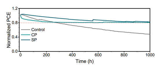
imageS 34 Compare the unencapsulated control groupCPandSPNormalization of devices in accelerated aging testingPCEChange over time.SPdevicePCESlowest decay rate, demonstrating optimal long-term stabilityButCPThe device showed significant performance degradation in the early stages of testing.
Other characterizations
1. angle resolutionXX-ray Photoelectron Spectroscopy(AR-XPS) Analyze the depth distribution and penetration ability of passivating agent molecules in perovskite thin films.confirmFIPA-SPPatterns can efficiently remove deep layersPEAIMinimize surface residue and enhance passivation repeatability.(image1d)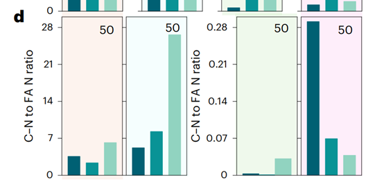
2. XX-ray diffraction(XRD) Analysis of the crystal structure changes of perovskite thin films after passivation treatment and2DFormation of phases.confirmFIPASignificant inhibitionPEAIPowder peak and2DPhase formation effectively suppresses the occurrence of phase transition.(image1e)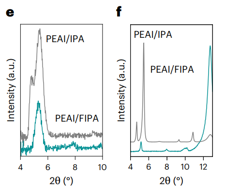
3. Photoluminescence spectrum(PL) Evaluate the suppression of non radiative composite losses,PLIntensity reflects the passivation effect of defects.displayFIPAHaving the ability to remove passivating agent molecules,IPAWhen the volume ratio increasesPLThe intensity gradually increases.(image3g)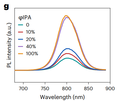
4. scanning electron microscope(SEM) Directly observe the surface morphology changes of perovskite thin films, especiallyPbI2Transformation status of enriched areas.confirmFIPAinhibitPEAIReactivity, after processingPbI2Enrichment area(Bright area)Some still exist.(image1g)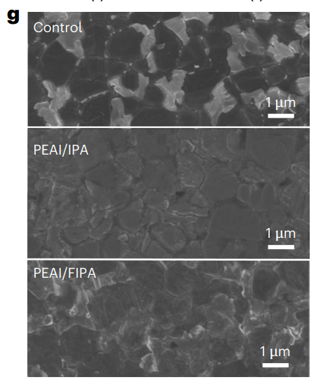
5. Nuclear magnetic resonance spectroscopy(NMR)and Fourier transform infrared spectroscopy(FTIR) Research on solventsPbI2Molecular interaction mechanism between passivating agent ligands.confirmFIPAFluorine atoms form strong hydrogen bonds with ammonium passivators, competitively hindering the formation of low dimensional phases.(image2f)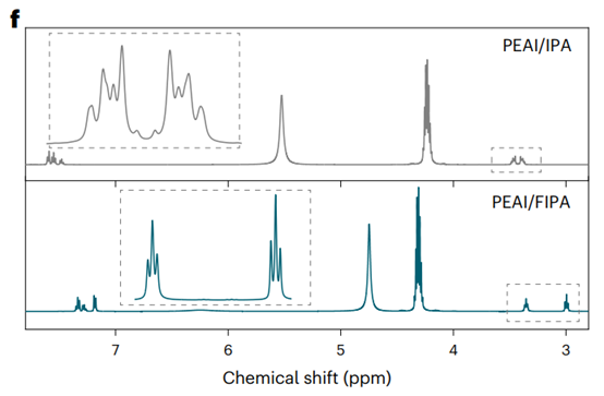
6. Statistical analysis of photovoltaic parameters : EvaluationSPThe universality, repeatability, and applicability of the strategy.confirmSPThe strategy performs excellently in various devices,1 cm2large areaPSCsofPCEfrom21.6%upgrade to24.5%.(imageS 24a)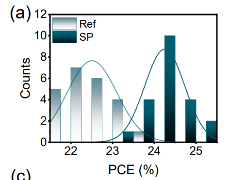
Conclusion
The research team has successfully developedSaturation passivation(SP)StrategyEffectively solvePSCsThe inconsistent effects caused by surface state variations in traditional passivation methods significantly improve device efficiency, stability, and reproducibility.
Core innovation breakthrough:
1. FIPAThe key role of solventsFluorinated isopropanol(FIPA)Significantly reduces the reactivity of passivating agent molecules with perovskite, compared to traditional isopropanol(IPA)Ensure defect passivation and do not interfere with charge transfer.FIPAExpand the operating window to make the strategy highly tolerant to changes in passivating agent concentration, deposition methods, and compatible passivating agents, demonstrating excellent versatility.
2. device performanceAchieving multiple efficiency breakthroughs:n–i–pLow bandgapPSCreach25.6%Thep–i–nLow bandgapPSCreach26%Thep–i–nwide bandgapPSCreach23%The1 cm2large areaPSCreach24.5%.SPStrategy provides a wider range of passivating agent concentration operations(20-100 mM PEAIStable efficiency maintained under concentration25%)Effectively suppressing hysteresis effects and significantly improving the performance of large-area devices.
3. Excellent stability performanceDuring accelerated life testing(65°C、0.8SunlightN2environmentSPdevice1000After hours, it still remains above80%initialPCEHowever, traditional passivation(CP)Device in front260Significant decline within hours, even worse than the untreated control group, attributed toSPThe strategy effectively reduces excessive penetration of passivators.
4. QFLSSignificant improvement:SPContinuous processing of thin film displayQFLSimprove,100 mM PEAI/FIPAProcessed filmQFLSfilmThe improvement is significant17.5 mVSignificantly better thanPEAI/IPAof12.8 mVIt demonstrates a reproducible effect in reducing open circuit voltage loss.
Reference from Nature Energy_DOI: 10.1038/s41560-025-01791-z
This article is rewritten by Enlitech for scientific research and academic sharing. If there is any infringement, please inform us by email