-
E-mail
qeservice@enli.com.tw
-
Phone
18512186724
-
Address
Room 409, Building A, No. 169 Shengxia Road, Pudong New Area, Shanghai
About Us
Guangyan Technology Co., Ltd
Date: 2025-09-01Read: 1
Research background and challenges
perovskite/Silicon stacked solar cells have become an important candidate for the next generation of photovoltaic technology due to their ability to break through the efficiency limit of single junction cells. Especially on industrialized textured silicon substrates, this technology demonstrates excellent light capture capability and cost-effectiveness, with good prospects for industrialization. However, its commercialization still faces key technological bottlenecks:
Core Challenge 1: Film Stability Issues in the Manufacturing Process
Mixed two-step evaporation-Although the solution deposition method can achieve conformal bonding with textured silicon substrate, the process requires high temperature(~150°C)And high humidity(~40% RH)Air annealing in the environment
This condition leads to severe decomposition of the surface of perovskite thin films due to the dual effects of high temperature and moisture
Core Challenge 2:PbI2The negative effects of by-products
Excess generated by film decompositionPbI2Formation of ion migration channels and degradation of accelerator components
More seriously, it triggers interface carrier recombination, resulting in loss of device efficiency and deterioration of stability
These process stability issues and the resulting performance degradation,Serious constraints on perovskite/The long-term stability and durability of silicon stacked batteries have become key technical barriers to large-scale industrial production.
Research team and significant achievements
This study was conducted byProfessor Tan Hairen and Professor Kong Wenchi from the State Key Laboratory of Solid Microstructure, Nanjing UniversityCo leadership, published in a journal《ACS Energy LettersHow to translateThe research team has successfully solved the problem of perovskite/The core challenge in the industrial process of silicon stacked batteries is:2Thin film decomposition caused by high-temperature and high humidity air annealing in the mixed two-step deposition method
PbI
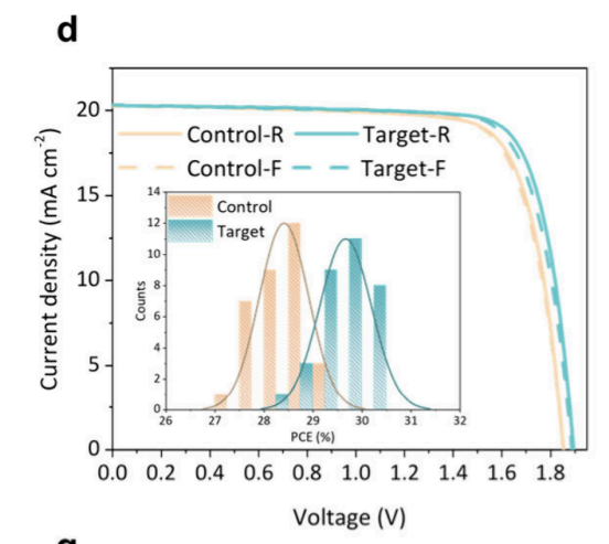
The issue of by-products.Fig. 4dThe key innovation of the team lies inintroduceDMPESIHydrophobic internal encapsulation layerEffectively suppressed the surface decomposition of perovskite during annealing, significantly reduced the non radiative recombination rate, optimized the quality of crystal growth, and thus improved the open circuit voltage and fill factor of the device. This willDMPESISuccessfully applied to mixed evaporation of textured substrates
-The solution deposition process has greatly expanded the application fields of this molecule.Industrial textured perovskite prepared by the team/Silicon stacked battery achieves30.49%1800Conversion efficiencyIn long-term stability testing, afterThe maximum power point tracking test for the hour still maintains the initial efficiency72384%,Maintaining initial efficiency after hourly wet heat testing
80%
These data far exceed the performance of the control group, fully demonstrating the significant effect of this method in improving device stability and durability. This technology is suitable for preparation in high humidity environments, laying a solid foundation for industrial large-scale low-cost production.
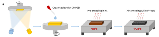
Experimental steps and processFig. 1aPreparation of high-performance and stable perovskite through sophisticated thin film deposition and additive strategies
/ Silicon stacked solar cells. The following are the main experimental steps:·Substrate preparation and bottom battery constructionSilicon heterojunction with industrialized texture4(SHJ)The bottom battery serves as the substrate. To prepare a stacked battery, the first step is toLaser cutting of silicon wafers into2.5 × 2.5 cm2The size, then proceed20200°CAnnealing is used to repair sputtering damage. Next, sputter onto the silicon substrateNano thick indium tin oxide
(ITO) As a composite layer.·Two step sedimentation method of perovskite layerThe preparation of perovskite thin films adoptsMixed two-step evaporation-
Solution deposition method .oFormation of inorganic skeletonFirstly, co evaporate on the substrate through thermal evaporationPbI2and540CsBr
, forming a covenant Nano thick inorganic skeleton layer.oOrganic salt solution spin coating andDMPESIaddSubsequently, the perovskite precursor will be included(asFA0.8Cs0.2Pb(I0.8Br0.2))Organic salt solutions, andKey stabilizers——DMPESISpin coat onto the formed inorganic thin film. thisDMPESIAdditives play a crucial role in solutions and can interact with
PbI2 Reaction forms a hydrophobic internal encapsulation layer.oPre annealing and air annealing:The film after spin coating will first be90°CPre annealing treatment is carried out in a nitrogen environment. Continuing with the critical air annealing step, around150°Cpeace treaty45%Relative humidity (or achieved in high humidity testing)2060%Annealing in an environment with relative humidityminute. This step is
DMPESI The key to forming a protective layer and inhibiting the decomposition of perovskite.·
Upper layer and electrode deposition After the preparation of the perovskite layer is completed, the electron transport layer and electrode will be deposited in sequence.20oFor single junction perovskite solar cells, the first step is thermal evaporationNano basedC60Thin film, then deposited through atomic layer(ALD) 15Nano based
SnO2 .oFor stacked solar cells, in50C60After the layer, there is sputteringNano based
ITO .oFinally, heat evaporated silver150(Ag)400As the top electrode (for single junction batteries)
Nano, stacked battery Nano).·Preparation of anti reflection layer(For stacked batteries100)To further enhance the light capture capability of the stacked battery, it will eventually undergo thermal evaporation on its surface2Nano based
MgF
As an anti reflection layer.Characterization methods and results
Quasi Fermi level splitting(Quasi-Fermi Level Splitting, QFLS)Evaluate the degree of non radiative recombination loss and defect passivation effect in perovskite thin films,QFLSImprove the open circuit voltage of directly related devicesVOCimprove. adopt405 nmLaser excitation source is introduced into the integrating sphere measurement system through optical fiber, and the laser intensity is adjusted to
1 SunMeasurement of photoluminescence quantum yield under equivalent conditions.DMPESIProcessing significantly improves the structure of each layerQFLSvalueAmong them, calcium titanium ore body materials are the main onesVOCThe source of loss is obtained after processingsignificantly improved.DMPESIEffectively suppressed surface decomposition during air annealing process,Reduce non radiative recombination at the interface, making perovskite/C60At the interfaceVOCThe losses are correspondingly reduced. By studying pure perovskite thin filmsHTL/Perovskite andHTL/perovskite/ETLSystematic comparison of three stack structures confirms

DMPESIThe processing exhibits excellent defect passivation ability on all interfaces.Figure 3dDisplay the extracted data from different stack structuresQFLSValue comparison.DMPESIProcessing group in pure perovskiteHTL/Perovskite andHTL/perovskite/ETLThe interfaces of each layerQFLSThe values were significantly higher than those of the control group, visually demonstrating its effectiveness in suppressing non radiative recombination losses, which strongly explains the device

VOCThe fundamental reason for improvement.Latest Release from Guangyan Technology
QFLS-MaperAnalyze the upper limit of material potential!Enlitech QFLS-MaperLet youCompetitive1/5cost advantageYou can obtain itQFLS MappingandQFLS
imagingClearly display the spatial distribution of quasi Fermi levels, making the quality of materials clear at a glance!
Track our updates and obtain them as soon as possibleNew technology information!
Electroluminescence quantum yield(EQEEL)Further analyze non radiative recombination of devices and quantify quasi Fermi level splitting in single junction solar cells. use
Keithley 2450The voltage source measurement unit provides a constant current density and measures the photons emitted from the device in all directions through an integrating sphere and a calibrated spectrometer.DMPESISignificant improvement in electroactive optical rotation performance through processing: Equivalent to1 SunUnder simulated current density conditions,DMPESIProcessing group componentsEQEELreach0.430%Significantly better than the control group0.145%. Corresponding toVOCThe losses are respectively142 mVand170 mV,DMPESItreatment groupVOCLoss reduction28 mVThis result indicates that

DMPESIBy suppressing surface decomposition and optimizing the crystallization process, better perovskite quality and lower non radiative recombination can be achieved, effectively improving the open circuit voltage of the device.Figure 3eDisplay Control Group andDMPESIProcessing group for perovskite devicesELSpectral comparison.DMPESItreatment groupELThe intensity is significantly higher than that of the control group, providing strong evidence
DMPESIEffectively suppressing non radiative recombination, allowing more charge carriers to emit light in the form of radiative recombination, exhibiting excellent carrier quality.current density-voltage
(J-V)Curve measurementEvaluate the photovoltaic performance parameters of solar cells, using single junction cells in nitrogen charging glove boxesKeithley 2400Measurement and use of stacked batteriesKeithley 2450Voltage source measurement unit, inEnliTech SS-X 3A
Solar simulatorMeasure under illumination in the air.DMPESIProcessing significantly improves device performanceThe optimal efficiency of single junction perovskite cells is achieved21.2%(VOC = 1.227 V,2JSC = 21.0 mA cm-,FF = 82.4%)The control group only20%And there is almost no forward scanning
J-VDelay phenomenon.Industrial textured perovskite/Breakthrough in Silicon Stacked Cells30.49%Laboratory efficiency, obtaining29.8%Certification efficiencyCompared to the control group29.05%The absolute efficiency improvement exceeds1%,VOCenhance40 mV,FFUpgrade nearby2%Statistical analysis shows thatDMPESIThe average efficiency of modified stacked batteries is improved compared to the control group

1.2%.Figure 3aShowcasing the best single junction perovskite cellsJ-VCurve comparison.
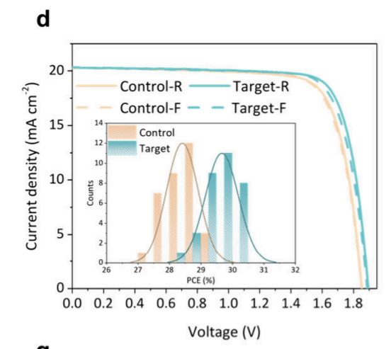
DMPESIThe curve shape of the processing group device is better, and the hysteresis phenomenon of forward and backward scanning is significantly reduced, confirming the stability and efficiency improvement of performance.Figure 4dPresenting the best stacked batteryJ-VCurve and efficiency distribution statistics.30DMPESI
The curve of the treatment group is significantly better than that of the control group, especially in terms of open circuit voltage and fill factor, with embedded graph statistics exceedingThe efficiency distribution of each device shows a significant improvement in the average efficiency of the processing group and a more concentrated data distribution.
External quantum efficiency(EQE)Measure the photons of the battery at different wavelengths-Electronic conversion efficiency and calculation of integrated photocurrent density. Single junction batteries equipped with lock-in amplifiers for use in airQESystem measurement, stacked batteries use wavelength850 nm(Bottom battery) and460 nm(Top battery) high brightness
LEDBias light is used for bias illumination measurement.DMPESIProcessing and improving spectral response characteristicsIn single junction perovskite cells,DMPESIThe integrated photocurrent density of the processing group reaches221.30 mA cm-Superior to the control group221.19 mA cm-The top sub cells of perovskite in stacked batteries20.67SHJThe integrated current densities of the bottom sub batteries areand220.25 mA cm
-The slightly higher current density design of the top sub battery aims to strategically introduce current mismatch and improve the performance and operational stability of stacked devices.On the textured substrate,DMPESIProcessing devices are available550 nm2The following bands show higher overall response, attributed to surface decompositionPbI
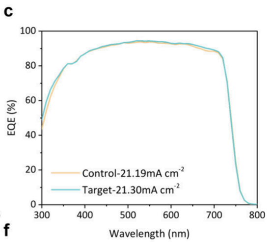
Reduced parasitic absorption.Figure 3cSingle junction perovskite cellEQECurve comparison.DMPESIThe processing group showed an improvement in spectral response, especially in the short wavelength region where it performed better and higher
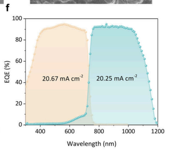
JSCThe values match.Figure 4fDMPESIProcessing stacked devicesEQECurve, including the response of perovskite top and silicon bottom sub cells. Two sub batteries
EQEThe curves overlap well and perform well in their respective absorption ranges, confirming excellent spectral allocation and current matching effects.Maximum power point tracking(MPPT) /
Operational stability(ISOS-L-1)Evaluate the long-term stability of the device under simulated sunlight. In the ambient air(30-50%Using multi-color in relative humidityLEDSimulators providedAM1.5G-2Standard lighting(100 mW cm)The operating temperature of the device is approximately35°C(Self heating), ambient temperature
25°CConduct packaging device testing without active cooling conditions.DMPESISignificant improvement in long-term operational stability through processing: Jing1800DMPESIModified stacked devices in the near futurehourMPPTMaintaining initial efficiency even after testing89084%The control group devices are only available inAfter hours, it rapidly degrades to an initial efficiency of about
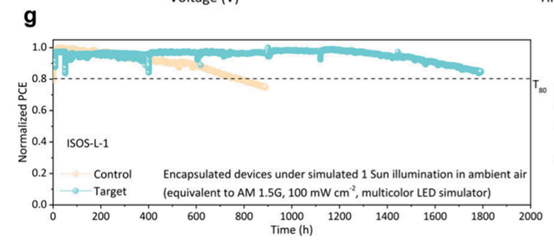
75%Show significant performance differences.Figure 4gShowcasing packaged stacked devicesAM1.5GFull spectrum simulation under sunlightMPPTracking results.
DMPESIThe efficiency of the processing group decays significantly slower over time compared to the control group, providing strong evidence of its operational stability performance.damp heat(Damp Heat) /
long-term stability(ISOS-D-3)Evaluate the long-term stability of the device in high temperature and high humidity environments. Place the packaged stacked devices in an environmental testing chamber and maintain a constant state85°Ctemperature and80085%30Relative humidity exceeds
Hour by hour, regularly measure performance (approximately)After cooling for minutes.DMPESIProcessing exhibits excellent resistance to moisture and heat: Jing723DMPESIModified stacked devices inMaintaining initial efficiency even after hour of wet heat testing33480%The durability performance is outstanding. The control group devices are inDegradation to initial performance after hours67%, Display
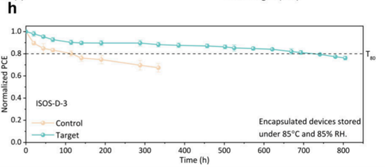
DMPESIThe protective effect in harsh environments.Figure 4hShowcasing packaged devices85°C/85% RHLong term stability test results under dark conditions.
DMPESI
The processing group showed a slower efficiency decay trend in high humidity and heat environments, once again confirming its excellent durability performance.Other characterizationsX
X-ray diffraction(XRD)Characterize the phase composition and crystal quality of perovskite thin films.DMPESIConcentration exceeds3 mg/mLAt that time7°3Formation of place1D DMPESPbI2Processing group thin films under extended annealing and high humidity exposurePbI

The generated amount is negligible, while the control group shows a significant increase.(Figure 1b)
scanning electron microscope(SEM)Observe the changes in film morphology and grain size.DMPESI

During the annealing process, the treated film only undergoes slight decomposition accompanied by significant grain growth, presenting a more uniform morphology and larger grains on textured substrates, while the control group experiences severe surface degradation.(Figure 2a)X
X-ray Photoelectron Spectroscopy(XPS)confirmDMPESIMolecular Introduction andPb-IChemical reconstruction of bonding environment.S 2pspectrum166.0 eVSignal confirmationDMPESIintroduce,Pb 4fandI 3dThe downward shift of the binding energy of the core energy level is attributed to1DIn the structurePb-I

The key length increases.(Figure 1d.e)
Flight time secondary ion mass spectrometry(TOF-SIMS)exploreDMPESI

Distributed spatially within the film. Additives are mainly enriched in the surface and bottom interface regions of the film, and their accumulation in vivo can be ignored, attributed to the steric hindrance effect of the conjugated ring structure of the aryl additive.(Figure 1f)
Time-resolved photoluminescence(TRPL)Measure carrier lifetime to evaluate non radiative recombination rate.DMPESISignificant extension of carrier lifetime in thin film processing1045.0 ns(Control group)515.8 ns)Prove effective reduction of non radiative recombination rate.
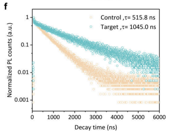
(Figure 2f)ultraviolet-visible
(UV-vis)absorption spectrumMeasure the absorption characteristics and optical bandgap of thin films.TaucImage displayDMPESIThe introduction did not cause significant changes in the bandgap of the thin film(Eg≈1.67 eV
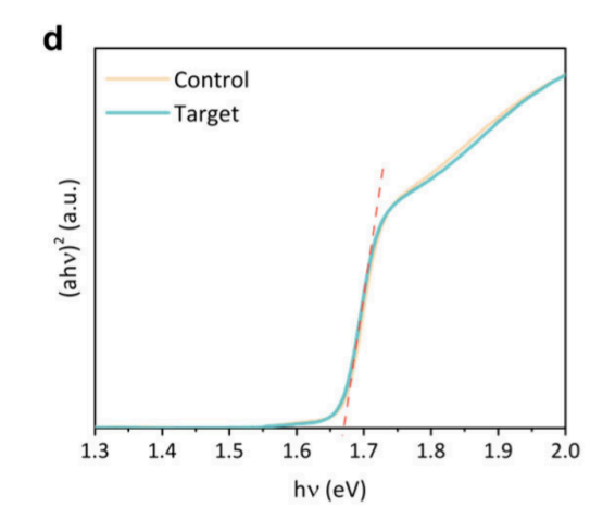
).
(Figure 2d)Contact angle measurementverifyDMPESI

The hydrophobicity of the treated film is enhanced. The processed film exhibits enhanced hydrophobicity during both pre annealing and air annealing stages.(Figure S9)
Stable power output(SPO)Measure the stable power of the device during long-term continuous operation.DMPESIImplementation of processing stacked devices30.3%

Stable power output.(Figure 4e)photo
/digital imageVisually display the physical appearance and humidity exposure degradation of the device.80% RHTesting in progress48DMPESIThe treatment group maintains the original color integrity for a long time, while the control group
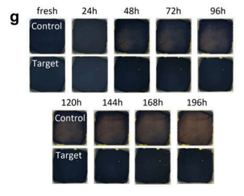
Obvious yellow decomposition points appeared within hours and extensively degraded.
(Figure 2g)ConclusionThe research team introducedDMPESIHydrophobic additiveSuccessfully solved the problem of perovskite
/Breakthrough achievements have been made in the core technology bottleneck of the industrial process of silicon stacked batteries.DMPESI2Molecules andPbI3Reaction formation1D DMPESPbIPerovskite forms a protective encapsulation layer at the interface, effectively suppressing thin film decomposition during air annealing. This mechanism promotes the formation of larger grains, reduces defect density, and significantly improves carrier lifetime(
1045.0 ns vs 515.8 ns)And enhance the stability of the film in high temperature and high humidity environments.Significant breakthrough in device performanceSingle junction perovskite cells achieve high efficiency21.2%Almost noneJ-VDelay phenomenon.Industrial textured perovskite/Silicon stacked battery sets a new record30.49%Laboratory efficiency record, obtained29.8%Certification efficiencyCompared to the control group, the absolute efficiency improvement exceeds1%,VOCenhance40 mV,FFUpgrade nearby
2%.1800Long term stability performance: Stacked devices inhourMPPTMaintain initial efficiency after testing72384%,Maintain after hour humidity test80%Efficiency far exceeds the performance of the control group. On the textured substrate,DMPESI2Processing devices exhibit better spectral response in the short wavelength region, confirming
PbIParasitic absorption is effectively reduced.This study aims to industrialize low-cost large-scale production of perovskite/Silicon stacked solar cells provide a feasible technological path,
Combining record breaking high efficiency and long-term operational stability, laying a solid foundation for the commercialization of stacked batteries
.