-
E-mail
qeservice@enli.com.tw
-
Phone
18512186724
-
Address
Room 409, Building A, No. 169 Shengxia Road, Pudong New Area, Shanghai
About Us
Guangyan Technology Co., Ltd
Date: 2025-08-06Read: 2
Research Background
The quality of buried interfaces has become a key technical constraint in the efficiency improvement process of perovskite stacked solar cells. This study delves into the technical bottleneck of buried interfaces in perovskite sub cells, aiming to address the core issues that affect the photoelectric conversion efficiency and long-term stability of stacked cells.
•Structural defects and chemical reactionsAt the buried interface of perovskite sub cells, there are harmful structural defects and chemical reactions that can lead to significant non radiative charge carrier recombination and harmful chemical reactions.
• PEDOT:PSSThe challenge brought by layers: the widely used hole transport layer currently(HTL) PEDOT:PSSIts acidity and hygroscopicity can cause adverse oxidation reactions, seriously deteriorating the operational stability of perovskite materials and their devices under high temperature and light exposure.
•Nanovoids and crystal defects:due toPEDOT:PSSThe possible spatial heterogeneity of the layer, as well as the rapid growth of tin lead perovskite, result in high-density morphological nano voids, crystal defects, unfavorable strain, and poor crystallinity at the buried interface. Especially on smooth substrates, it is easy to form visible "white spots" to the naked eye.
•Research challenges of buried interfaces:Compared to the top-level interface, the buried interface of the perovskite layer is relatively difficult to access in devices and has been less studied.
Research team and research focus
This study was conducted byChen Wei and Liu Zonghao from Wuhan Optoelectronics National Research Center of Huazhong University of Science and Technology, and Oxford University in the UKHenry J. SnaithProfessor leadership,Published in the top issue《Nature communications》. Mainly through designing aThiol functionalized mesoporous silica layer(MSN-SH)As a buried interface of perovskite thin filmssuperstructureTo solve the problem of harmful structural defects and chemical reactions at the buried interface of neutron cells in series photovoltaic devices. This method aims to regulate the properties of perovskiteCrystallization process, elimination of nanopores, passivation defectsAnd suppress the formation of tin lead perovskite thin films Sn(II)The oxidationThis significantly reduces carrier losses and improves the stability of the device.
Key research achievements
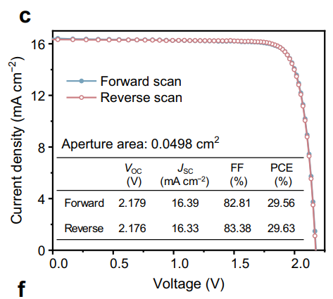
Fig4c
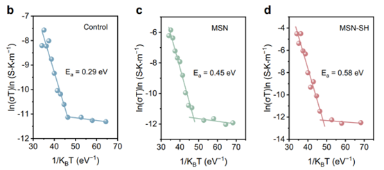
1. Breakthrough in Interface Optimization TechnologyMSN-SHThe layer achieves interface improvement through multiple mechanisms: significantly enhancing the wettability of perovskite precursors, effectively eliminating nanovoids and film formation defects; Significantly release residual strain of the film (from)72.2 MPadrop to4.6 MPa)And enhance crystallinity; Using thiol groups to passivate defects and inhibitSn(II)Oxidation and removal of ion migration barriers0.29 eVupgrade to0.58 eVAt the same time, increase the adhesion strength of the interface from0.26 MPaEnhance to0.67 MPa.
2. Breakthrough in efficiency and performance Narrow bandgap tin lead perovskite single junction battery achieved23.7%Best efficiency (average)23.1%), open circuit voltage0.89 VImplementation of fully perovskite layered battery29.6%Best efficiency,Certification efficiency29.5%Steady-state efficiency28.7%,Set a new performance record for single ended stacked batteries;11.3 cm2Stacked mini modules achieve high efficiency24.7%Show excellent amplification potential.
3. Significantly improved stabilityNBGSingle junction batteries85°CAging in dark nitrogen environment164Maintain after hours85%Initial efficiency; Encapsulated stacked batteries1Under the sunlightMPPTtest445Maintain after hours90%Efficiency; Stacked devices in85°Caging150Still retained after hours82%初始性能。
4. Technical universality verificationMSN-SHThe processing strategy also applies to lead based wide bandgap perovskites, making1.77 eVBattery efficiency reaches20.6%And effectively suppress the photo induced halide segregation phenomenon of mixed halide perovskites.
Experimental steps and process
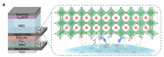
Fig1a
The core strategy of this study is to introduce a thiol functionalized mesoporous silica layer at the buried interface of perovskite(MSN-SH)As an interface modification layer, its effectiveness is verified through systematic component preparation and performance comparison.
Preparation process of single junction battery: The standard process includesITO/Glass substrate cleaning, hole transport layer(PEDOT:PSSorMe - 4PACz)Spin coatingcriticalMSN-SHDispersion liquid spin coating and annealing treatmentContinuing with the deposition of perovskite precursor solution, thermal annealing, and surface passivation layer(EDAI2orPDAI2)Process, and finally heat evaporate the electron transport layer(C60TheBCP)With silver electrodes.
Preparation of stacked batteries: Adopting a layered construction strategy, first complete the preparation of wide bandgap sub cells, and then construct them through atomic layer deposition technologySnOxReorganize the interface, and finally deposit the functional layers of narrow bandgap sub cells in sequence to form a complete two end stacked structure.
Modular verification: Laser engraving process is performed on a large-area substrate to form multiple series connected sub battery cells, and interconnection and packaging are completed to verify the industrialization potential of the technology.
Comparison and verification methods: Systematic comparison between introduction and non introductionMSN-SHQuantitatively evaluate the improvement effect of components in terms of photoelectric conversion efficiency, stability, and interface characteristics.
Characterization methods and results
Quasi Fermi level splitting(QFLS)Quantum efficiency of photoluminescence(PLQY)
Evaluate the open circuit voltage potential and non radiative recombination loss of perovskite thin films, based onPLQYResult CalculationQFLSValue.
MSN-SHEffectively reduce processingPEDOT:PSSLayer interface loss significantly improves the optoelectronic properties of thin films.PEDOT:PSS/MSN-SH/The perovskite stackPLQYFrom the control group0.885%Significantly improved to5.586%, corresponding toQFLSValue from0.856 eVincrease to0.903 eV, demonstrating excellent voltage potential enhancement effect.
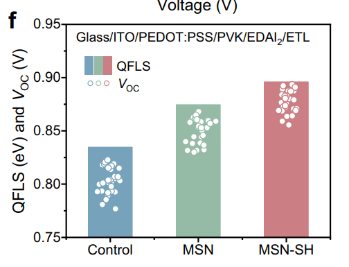
Fig. 3fBy comparing the actual voltage with the theoretical voltage potential, the quantification was carried outMSN-SHThe effect of interface improvement on improving the open circuit voltage of perovskite solar cells
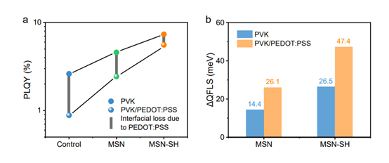
FigS. 30a, 30bDisplay different stack structures separatelyPLQYandQFLSData comparison.MSN-SHThe sample was significantly better than the control group in both indicatorsMSNThe sample confirms its significant effect in suppressing non radiative recombination and enhancing open circuit voltage potential.

Guangyan Technology has launched a new productQFLS-MaperPredict material performance limits!
Enlitech QFLS-MaperIn an economically affordable manner1/5investment cost, can be achievedMappingfunctionAnd generateQFLSimageVisually present the full distribution of quasi Fermi levels, and immediately demonstrate the quality of the material!
Follow us and master first-hand technical information!
current-voltage(J-V)Characteristics and photoelectric conversion efficiency testing
Evaluate the basic electrical performance, photoelectric conversion efficiency, and hysteresis phenomenon of the device.
MSN-SHSignificant performance improvements have been achieved on various types of batteries:
Narrow bandgap(NBG)Tin lead perovskite single junction battery:,MSN-SHModified device averagePCEreach23.10%Compared to the control group19.64%Significantly increased. Best Device Implementation23.74%PCE (VOC 0.887 V, JSC 32.77 mA cm-2,FF 81.67%)And the hysteresis phenomenon is almost negligible.
wide bandgap(WBG)Perovskite single junction battery:Demonstrating good universality,1.77 eVdevicePCEGundam20.60%(VOC 1.330 V, JSC 18.29 mA cm-2,FF 84.69%)The efficiency of third-party authentication is20.27%.
Full perovskite stacked devices:Benefiting from the synchronous optimization of twin batteries, the averagePCEreach29.16%Best Device Implementation29.63%PCE (VOC 2.176 V, JSC 16.33 mA cm-2, FF 83.38%). JingSIMITthird-party certificationPCEfor29.50%Steady-state efficiency28.7%.

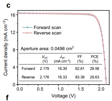
Fig. 3c, Fig. 4candFigS. 37Display single junction and stacked devices separatelyJ-VFeatures that exhibit extremely low hysteresis and excellent optoelectronic performance.
External quantum efficiency(EQE)test
Evaluate the photoelectric conversion efficiency of the device at different wavelengths and calculate the integrated short-circuit current density. useEnlitech QE-RQuantum efficiency measurement systemWhen testing in ambient air, the stacked devices are measured separately850 nmand460 nmhigh brightnessLEDtoWBGandNBGThe sub battery is biased.
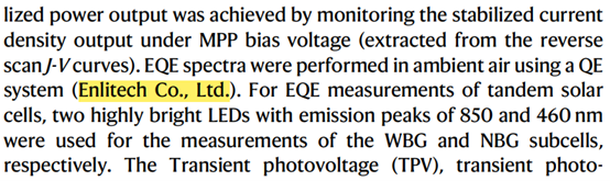
MSN-SHEffectively improving the quantum efficiency performance of devices.NBGTin lead perovskite single junction batteryEQEThe spectrum has improved throughout the entire wavelength range, especially in the long wavelength region where the response is enhanced and integratedJSCFrom the control group31.42 mA cm-2upgrade to32.35 mA cm-2.
The all perovskite stacked devices exhibit excellent spectral matching characteristics,WBGSub battery integrationJSCfor16.26 mA cm-2,NBGThe sub battery is16.02 mA cm-2The two have highly matched current densities and complementary spectral response ranges, laying the foundation for achieving high-efficiency stacked structures.
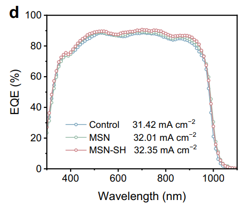
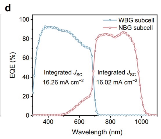
Fig. 3dandFig. 4dDisplay single junction and stacked devices separatelyEQESpectral comparison, clear presentationMSN-SHThe significant effect of processing in improving the efficiency of light collection and charge extraction.
External quantum efficiency of electroluminescence(EQEEL)
Quantify the degree of non radiative recombination loss of devices, andVOCPerformance is closely related. useEnlitech ELCT-3010(REPS)systemMeasure and inject current density set close to the short-circuit current density under sunlight.
MSN-SHProcessing of DevicesEQEELGenerate significant improvement effects. ApproachingJSCUnder the condition of current injection, the deviceEQEELValue from the control group0.20%Significantly increased to2.61%, with an increase of13timesThis significant improvement directly confirmsMSN-SHEffectively suppress non radiative recombination processes within the device.
The corresponding non radiative composite loss is reduced by about70 mV, with devicesVOCThe actual improvement is highly consistent and verifiedEQEELThe reliability of test results andMSN-SHThe effectiveness of interface modification strategy.
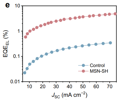
Fig. 3eDisplay the control group andMSN-SHdeviceEQEEL-Comparison of current density relationship,MSN-SHThe device exhibits significant advantages throughout the entire current range, especially in low current density regions.
open-circuit voltage(VOC)Loss analysis
Quantitative analysis based on detailed balance theoryVOCLoss components, including non ideal onesEQEAccurately locate the reasons for device voltage deviation from theoretical limits, including losses, secondary bandgap radiation recombination losses, and non radiation recombination losses. The analysis is based on actual measurementsVOCTheEQEELUse key parameters as input for calculation.
MSN-SHSignificant reduction in device total processingVOCLoss. The most critical improvement comes from a significant reduction in non radiative composite losses, as seen in the control group160 mVdrop toMSN-SHsample94 mVThe reduction rate has reached41%This result is consistent with the actual deviceVOCImprove height matching, confirmMSN-SHThe key role in suppressing non radiative recombination.
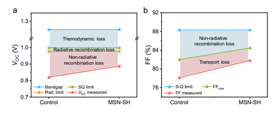
FigS. 29aDetailed comparison between the control group andMSN-SH NBGVarious aspects of batteriesVOCLoss components, clearly displayedMSN-SHThe device has significant advantages in reducing non radiative recombination losses.
Transient photocurrent(TPC)Transient photovoltaic voltage(TPV)
Explore the extraction and recombination dynamics of charge carriers within the device, and evaluate the impact of interface modifications on charge transfer pathways.
MSN-SHProcess synchronous improvement of charge extraction and inhibition recombination. Device current decay lifetime from the control group3.86 µsshorten to2.37 µsProve that the extraction speed of charge carriers is accelerated; Voltage decay life from149 µsextend to626 µsReflecting the effective suppression of charge recombination.
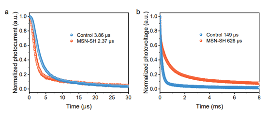
FigS. 26a, 26bDisplay separatelyTPCandTPVComparison of attenuation curves,MSN-SHDevices inTPCThe attenuation is faster in the test,TPVThe attenuation is slower in the test, clearly verifying the dual effect of buried interface modification in promoting charge extraction and suppressing interface recombination.
Operational stability(MPPT)test
Evaluate the long-term operational stability of the device under continuous illumination with maximum power point bias.
MSN-SHProcessing significantly improves the long-term stability of the device. UnpackagedNBGSingle junction battery continuous operation450hourMaintain afterwards93%Initial efficiency, far superior to the control group370After hours68%Encapsulation of fully perovskite stacked devices430hourAfter continuous operationmaintain90%The above efficiencySignificantly surpassing the control group325After hours75%Performance.
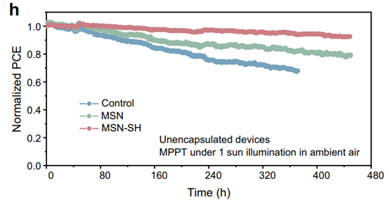
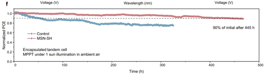
Fig. 3h, Fig. 4fDisplay single junction and stacked devices separatelyMPPTStability curve,MSN-SHThe device exhibits long-term operational stability in both configurations, confirming its excellent potential in practical applications.
Other characterizations
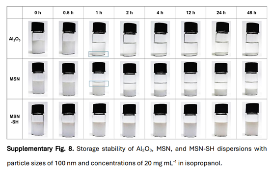
Stability testing of dispersed liquid storage Evaluate the stability of nanoparticle dispersion during storage and its impact on the processing window of device preparation.MSN-SHDispersed liquid in48No settling phenomenon after hours, significantly better thanAl2O3of1Hourly precipitation.(FigS. 8)
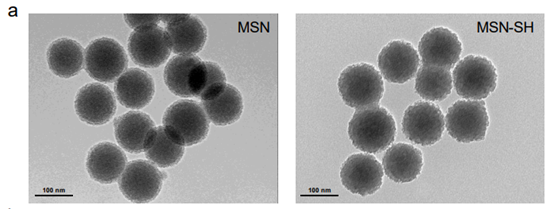
Characterization of Nanoparticle Characteristics comprehensive analysisMSNandMSN-SHThe physical dimensions, pore structure, and successful functionalization.MSN-SHReduce particle size to100 nm,FTIRandRamanSpectrum in2569and2563 cm-1Confirm successful grafting of thiol groups.(FigS. 10a)
Wettability and nucleation testing 研究MSN-SHThe influence on the wetting behavior of perovskite precursor solution.Contact angle from22.6°drop to12.7°Significantly improve wettability and promote heterogeneous nucleation.(FigS. 11)

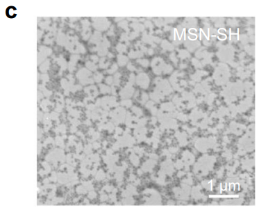
Film morphologySEMObserve the surface and buried interface morphology of perovskite films to determine the presence of nanocavities.MSN-SHThe base film presents a dense crystalline region without nano voids, which is in contrast to the control group's dome shaped voids.(Fig. 1c)
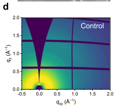
crystallinityGIWAXSanalyze Evaluate the crystallinity of perovskite films near buried interfaces.MSN-SHThe base film exhibits stronger diffraction intensity at all incident angles, higher crystallinity, and lower degree of amorphous phase.(Fig. 1d)
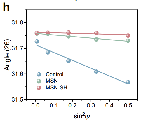
residual strainGIXRDtest Evaluate the residual stress state in perovskite thin films.MSN-SHEffectively reducing tensile stress from72.2 MPadrop to4.6 MPaSignificantly release film strain.(Fig. 1h)
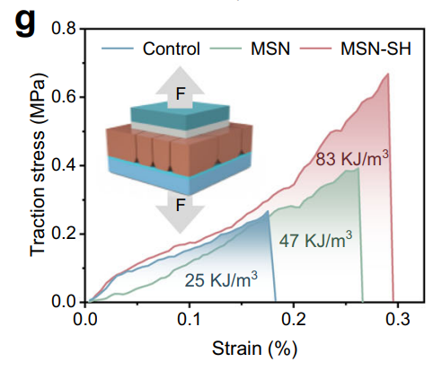
Mechanical strength testing verifyMSN-SHEnhancing the mechanical durability of buried interfaces.The critical tensile strength ranges from0.26 MPaupgrade to0.67 MPaCompared to fracture energy25Increase to83 kJ m-3.(Fig. 1g)
Comprehensive analysis of interface stability throughDFTCalculation, temperature dependent conductivityUV-VisandXPSExplore stability mechanisms in depth.Ionic migration activation energy from0.29 eVupgrade to0.58 eV,Sn(IV)Significantly reduced content, effectively inhibiting degradation.(Fig. 2b)
Time dependence of halide segregationPLtest Evaluate the phase segregation phenomenon of mixed halide perovskite under long-term illumination.MSN-SHModifying the film during exposurePLMaintain good shape and effectively suppress halide segregation.(FigS. 38c)

Conclusion
The research has been successfully developedThiol functionalized mesoporous silica layer(MSN-SH)As a superstructure modification layer for buried interfaces in perovskite solar cells, it significantly improves the efficiency and stability of perovskite stacked solar cells.
Core technological breakthrough:
Interface quality optimizationaspect,MSN-SHEffectively regulate the crystallization process of perovskite, eliminate nanovoids and passivate defects, while suppressingSn(II)Oxidation significantly reduces carrier loss. Mechanical strength from0.26 MPaupgrade to0.67 MPaResidual tensile stress72.2 MPadrop to4.6 MPaThe activation energy for ion migration is from0.29 eVRaise to0.58 eV.
Device performanceIn terms of efficiency, tin lead perovskite single junction cells achieve23.7%The realization of a fully perovskite layered battery29.6%Efficiency (certification)29.5%, steady state28.7%)Ranked among the top performers in single ended stacked batteries.11.3 cm2Stacked mini modules achieve high efficiency24.7%Showcasing excellent industrialization potential.
long-term stabilityIn terms of packaging, stacked batteries are1Sunlight illuminationMPPTtest445hourMaintain afterwards90%The above initial efficiency,85°Cthermal aging150hourStill maintained afterwards82%Performance far exceeds that of the control group.
Technical universalityObtain verification,MSN-SHThe strategy also applies to lead based wide bandgap perovskites,1.77 eVBattery efficiency reaches20.6%And effectively suppress the segregation phenomenon of mixed halides.
Reference from Nature Communications_SOI: 10.1038/s41467-025-59891-Z
This article is rewritten by Enlitech for scientific research and academic sharing. If there is any infringement, please inform us by email