-
E-mail
qeservice@enli.com.tw
-
Phone
18512186724
-
Address
Room 409, Building A, No. 169 Shengxia Road, Pudong New Area, Shanghai
About Us
Guangyan Technology Co., Ltd
Date: 2025-07-23Read: 1
Research background and difficulties

Although perovskite solar cells have developed rapidly, theirOpen circuit voltage still significantly lags behind theoryShockley–QueisserlimitBecoming a key bottleneck restricting efficiency improvement. The main reasons for voltage loss include:Mismatch of energy layers and excessive non radiative recombination at critical interfacesEspecially in traditional structures,SnO2Uncoordinated surface of electron transport layerSn2+ (Sn–OH)Forming shallow trap sitesSerious damage to electronic transmission efficiency. These interface defects not only reduce device performance, but also accelerate the degradation of perovskite in hot and humid environments, leading to insufficient long-term operational stability.
Research team and significant achievements
This groundbreaking study was conducted byProfessor Li Gang from The Hong Kong Polytechnic University(Gang Li) TheKuan LiuProfessor andJinyao Tang教授Co led by Hong Kong University of Science and Technology Guangzhou andMILES HKU-SIRICollaboration among scholars, published in journals《Advanced MaterialsHow to translate,InSnO2/Successfully constructed a self-assembled amphiphilic phosphonate derivative at the buried interface of perovskite(MeOBTBT-POEt)As a template driven by perovskite crystallizationTheir innovative methods are not onlyAccurately regulated the growth of perovskite crystalsAt the same time, it is also effectivePassivation of interface defects and optimization of energy level alignmentIt fundamentally solved the problem
VOC
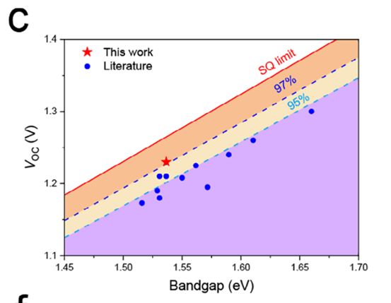
The problem of losses.Summary of Key Research AchievementsBreakthrough in device performance and ultra-low voltage loss:The research team has successfully developed perovskite solar cells(PSC)ofOpen circuit voltage increased to1.23 VVoltage loss only0.306 V,Reaching the theoretical limit97.2%—This is an extremely low loss value among all perovskite systems. The device has been implemented25.34%Power conversion efficiencyAfter testing with a standard solar simulator,
J-VThe curve shows no significant hysteresis effect.Long term stability:Under rigorous testing conditions(65°C、50%Relative humidity),PSCof1200T92Exceeding lifespan
hourSignificantly improved long-term operational stability in hot and humid environments.Accurate crystal orientation control:MeOBTBT-POEtThe template forms a highly oriented supramolecular structure through self-assembly,Inducing highly preferred formation of perovskite(100)crystal orientation.GIWAXSThe test confirmed this optimization orientation,DFTCalculation display template and(100)The bonding energy of the crystal surface is as high as
-0.94 eV.Efficient interface defect passivation and energy level alignment:MeOBTBT-POEtmoleculeActive passivationSnO2Oxygen vacancies and perovskitesPb2+defectIts high dipole moment(1.89 D)Coordinate interface energy level alignment and extract electron energy barriers from0.24 eVdrop to-0.03 eV.XPSThe results confirmed strong coordination interactions,PV-SCLCMeasurement shows trap state density from1.02×10^16drop to
0.66×10^16 cm^-3.
Carrier dynamics optimization:This strategy significantly suppresses non radiative recombination and achieves ultra-low voltage loss. Key manifestations include:Electroluminescence external quantum efficiency(ELECTION)from2.73%upgrade to10.29%Non radiative voltage loss from93.1 mV
drop to58.8 mVPhotoluminescence quantum yield(PLQY)from9.09%
upgrade to27.06%Quasi Fermi level splitting(QFLS)Analysis shows energy loss from62 meV
drop to34 meVTRPLMeasurement confirms an improvement in electronic extraction efficiency,
TPV/TPC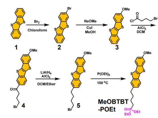
Measurement confirms reduction of carrier recombination and enhancement of transmission efficiency
1.Experimental steps and processFigure S1
Successfully synthesized key interface regulatory moleculesMeOBTBT-POEtThe research team successfully synthesized amphiphilic phosphonate derivativesMeOBTBT-POEtThe molecule is composed of rigid benzothiophene[3,2-b]Benzothiophene
2.(BTBT)Composed of a skeleton and flexible phosphonate alkyl tail, it exhibits excellent self-assembly properties.verify
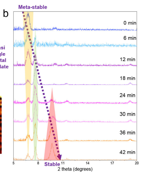
MeOBTBT-POEtSelf assembly characteristics and stabilityObtained by solvent evaporation methodMeOBTBT-POEtSingle crystal and analyze crystallographic data.Thermogravimetric Analysis(TGA)Evaluate thermal stability,Differential scanning calorimetry(DSC)Verify the assembly characteristics of room temperature metamolecules.in situXX-ray diffraction(XRD)
3.spectrum
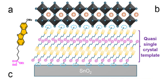
Monitor the crystal structure evolution of the thin film during thermal annealing and confirm that the molecule can spontaneously assemble to form a highly ordered two-dimensional single crystal morphology template at room temperature.Establish the theoretical basis for the interaction between molecules and perovskite crystal facesapplydensity functional theory(DFT)calculateevaluateMeOBTBT-POEtandFAPbI3Perovskite on different crystal planes((100)、(110)、(111))The interaction between it and(100)Crystal planes have interactions. ThroughDFTCalculate electrostatic potential
4.(ESP)
Evaluate the molecular dipole moment and demonstrate its potential for interface modification.Preparation of high-performance perovskite solar cellsAccording to the standardn-i-pstructure(FTO/SnO2/MeOBTBT-POEt/perovskite
/spiro-OMeTAD/Au)Preparation of devices:Substrate andSnO2 ETLpreparation:FTOGlass cleaning and UV radiation-After ozone treatment, spin coatingSnO2Solution,60200°C
annealingminuteMeOBTBT-POEtInterface decorationPut different concentrations in the glove boxMeOBTBT-POEtSpin coat chlorobenzene solution onto
SnO2 ETLupSedimentation of perovskite layer: PreparationCs0.03(FA0.97MA0.03)0.97Pb(I0.97Br0.03)3precursor solution(bandgap~1.53 eV)After spin coatingControlled humidity(20-30% RH)in the environment60100°C
annealingminuteHTLPreparation of electrodes: Spin coating in sequenceBABrandspiro-OMeTADSolution,10100°CannealingminuteFinally, thermal evaporation deposition80 nmthick
Au
electrode
Figure 1aCharacterization Techniques and ResultsQuasi Fermi level splitting(QFLS)And photoluminescence quantum efficiency
(PLQY)Characterization and ResultsPLQYIt is an indicator of the behavior of solar cells under open circuit conditions,PLIt is crucial to achieve higher photovoltaic voltage.QFLSAnalysis for in-depth exploration of charge recombination andV_OCLoss mechanism. measurementSnO2/The photoluminescence intensity of perovskite semi layered samples, and according to the formulaQFLS = qV_OC,rad + k_BTln(PLQY)Calculate the quasi Fermi level splitting. sutraMeOBTBT-POEtmodifiedSnO2/Half layered perovskite samplePLQYSignificant improvement, from9.09%increase to27.06%Corresponding energy lossΔ(V_OC,rad - QFLS)from62 meVSignificantly reduced to34 meV.QFLSAnalysis confirms that,ultra-lowV_OCThe losses are mainly attributed toSnO2/

Effective elimination of non radiative recombination at the buried interface of perovskite.image4dDisplayed with or withoutMeOBTBT-POEtmodifiedSnO2/Photoluminescence quantum efficiency of perovskite semi layered samples(

PLQY).image4eDisplayed the control group andBIMQuasi Fermi level splitting of components(
QFLS)Analysis results.tableS5summarized


V_OCLoss analysis.Latest Release from Guangyan Technology
QFLS-MaperAnalyze the upper limit of material potential!Enlitech QFLS-MaperLet youCompetitive1/5cost advantageBy doing so, one can acquire the ability to map spatial distribution andQFLS
imaging technologyClearly display the spatial distribution of quasi Fermi levels, making the quality of materials clear at a glance!
Track our updates and obtain them as soon as possibleTechnical information!current-Voltage(
J-V)CurvestandardAM 1.5 GUnder illumination, useEnliTechofSS-XSolar simulatorMeasure and perform forward and reverse scanning(1.25to-0.2 V)Evaluate hysteresis effect, delay time100 msTesting area

0.04 cm2.Buried interface modification(BIM)The performance of perovskite solar cells has significantly improved,The maximum power conversion efficiency reaches25.34%, open circuit voltage1.23 VShort circuit current density225.10 mA cm-Fill factor82.28%Control group devicesPCEfor22.81%, open circuit voltage1.197 VShort circuit current density225.08 mA cm-Fill factor
75.99%.For bandgap1.536 eVThe perovskite,Voltage loss only0.306 VReaching the theoretical levelShockley–Queisserlimit97.2%.J-VMeasurement display

No significant hysteresis effect.image4a:The control group showed the best performance(Control)And embedded interface modification(BIM)Components'
J-V1 Curve.
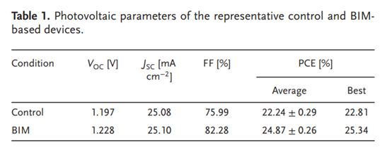
tableSummarized its photovoltaic characteristics.External quantum efficiency(
EQE)Spectral analysisuseEnlitech QE-RsystemMeasure the photons of the device at different wavelengths-Electronic conversion efficiency, using210 HzChopped monochromatic light, wavelength range300-850 nmThe short-circuit current density remains constant at different concentrations225.1 mA cm-, withEQEThe spectral integration values are highly consistent(error<1%). ThroughEQEThe first differential calculation of the spectrum is obtainedFAPhotovoltaic bandgap of perovskite based materials(E_gPV)approximately

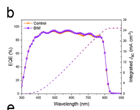
1.536 eV.image4bDisplayed the control group andBIMThe components of the group
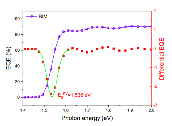
EQESpectrum.imageS26Further display
EQEThe first derivative of the spectrum is used to determine the bandgap of photovoltaics.
External quantum efficiency of electroluminescenceEQEELQuantifying the performance of perovskite solar cells under forward biasLEDNon radiative composite losses during operation, used for analysisV_OCLoss mechanism. useEnliTech LQ-100Photoluminescence quantum efficiency measurement systemTake measurements.BIMComponents in225.1 mA cm-Under injected currentEQE_ELSignificantly improved to10.29%, much higher thanThe control group2.73%. Corresponding toNon radiative composite losses from93.1 mVSignificantly reduced to58.8 mV, withJ-VDuring testingV_OCThe consistent improvement results prove the strategyEffectively suppressedSnO2/Non radiative recombination at the buried interface of perovskiteThis is achieving ultra-low


V_OCThe key mechanism for losses.imageS27displayedEQE_ELAs a function of injected current density, used for the control group andBIM
Group components.Long term operational stability testing(
ISOS-L-3)Evaluate the long-term operational stability of perovskite solar cells under thermal and humidity stress, and assess the commercial feasibility of the devices. sutraBIMThe processed components are122865°CoperationAfter hours, it still maintains its initial statePCEof92%
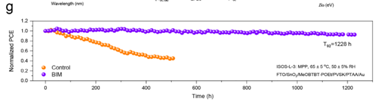
aboveSignificantly better than the control group. This enhanced stability is attributed to the effective elimination of shallow defects and moisture resistance.image4gDisplayed inISOS-L-3Under certain conditions, the control group and
BIM
The long-term operational stability test results of the components.Other characterizations•XX-ray photoelectron spectroscopy(XPS):2研究SnOElectronic transport layer(ETL)The chemical environment and interactions between the buried interface and perovskite.2Confirmed YesSnO2Medium oxygen vacancies and uncoordinated in perovskitePb+The spontaneous passivation effect of defects. (Image)3aThebThe
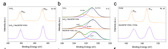
c)•Ultraviolet photoelectron spectroscopy(UPS):Evaluate the band structure at the electronic selective interface. sutraMeOBTBT-POEt2After modification,SnOThe work function is derived from4.16 eVMove up to3.82 eVElectronic extraction energy barrier from0.24 eVdrop to-0.03 eV.(Image)3dThe

e)•Time-resolved photoluminescence(TRPL):Study the kinetics of interface charge transfer and the efficiency of charge separation and extraction. The carrier lifetime of modified perovskite varies from381.7 nsshorten to183.9 nsConfirm the improvement of electron extraction efficiency.(Image)

3f)•Grazing incidence wide-angleXRay scattering(GIWAXS):Analyze the crystal orientation of perovskite thin films. Modified perovskite(100)Crystal planes are highly concentrated along the out of plane direction to achieve optimal orientation growth(Image)2bThe

c)•Density functional theory(DFT)Calculation:Estimate the interaction strength between molecules and different crystal planes of perovskite.MeOBTBT-POEtand(100)Crystal surface bonding(-0.94 eV)The molecular dipole moment is1.89 D.(Image)2dThe
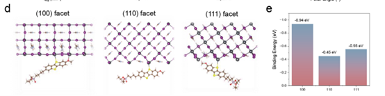
e)•XX-ray diffraction(XRD)Spectrum:Monitor the evolution of molecular thin film crystal structure and perovskite orientation. in situXRDConfirmed solid-Solid phase transformation process, after modification5.87(100)/(111)8.65Peak intensity ratio fromIncrease to.(Image)
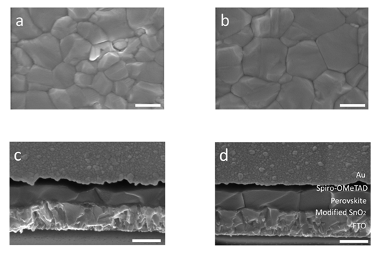
1b)•Scanning electron microscope(SEM):Observe the morphological characteristics of perovskite thin films. The larger size of the modified perovskite crystal domain is attributed to the delayed crystallization process on the hydrophobic surface.(Image)
S18)•light intensity-Open circuit voltage relationship:Determine the ideal factor and composite mechanism of the device.1.12BIM1.38The ideal factor of the device is reduced to(Control group))The charge recombination behavior is closer to the ideal state.(Image)

S29)•Transient photovoltaic voltage/Photoelectric current(TPV/TPC):Reveal the dynamics of carrier recombination and transfer.TPVAttenuation time from61.87 μsextend to133.34 μs,TPCAttenuation time from0.86 μsshorten to0.73 μs.(Image)
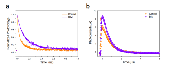
S30)•Pulse voltage-Space charge limited current(PV-SCLC):16 Estimate the electron trap density in perovskite. Trap state density from1.02×103cm-16drop to0.66×103cm-Significantly reduce trap states.(Image)
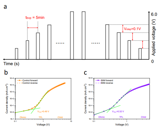
S31)•Mott-Schottky analysis and thermal conductivity spectroscopy(TAS):Quantitatively estimate the trap state energy level distribution and built-in voltage. Built in voltage from1.06 Vupgrade to1.10 VThe density of deep level trap states decreases by an order of magnitude.(Image)4fThe

S32
)ConclusionThe research has been successfully developedBuried interface regulation strategy, using self-assemblyAmphoteric phosphate ester derivativesMeOBTBT-POEt2InSnO
/Constructing crystal driven templates at the perovskite interface significantly improves the performance of perovskite solar cells.•Device performance:Research team implementation25.34%Power conversion efficiency and1.23 Vopen-circuit voltageFor1.536 eVBand gap perovskite, with only voltage loss0.306 V,Reaching the theoretical limit
97.2%.•Precise crystallization control and carrier optimization:Highly oriented supramolecular templateInducing preferential formation of perovskite(100)Out of plane orientationPromote vertical charge transfer.MeOBTBT-POEtof1.89 DDipole moment coordination interface energy level alignment,Electronic extraction energy barrier from0.24 eVdrop to-0.03 eVThe carrier lifetime varies from381.7 nsshorten to
183.9 ns.•Efficient interface defect passivation: This strategy2Active passivationSnO2Oxygen vacancies and perovskitePb+defectSignificantly inhibit non radiative recombination. Electroluminescence external quantum efficiency from2.73%upgrade to10.29%The photoluminescence quantum efficiency9.09%Increase to27.06%16The trap state density1.02×1016drop to0.66×103cm
-.•Excellent long-term stability:In hot pressing(65°C)And moisture(50% RH)92Under certain conditions, the device1200TExceeding lifespan
hour
Attributed to effective defect elimination and excellent moisture resistance.