-
E-mail
marketing@dymek.com
-
Phone
13917837832
-
Address
Room 306-308, Building 6, No. 35, Lane 2216, Jingao Road, Pudong, Shanghai
Daimei Instrument Technology Service (Shanghai) Co., Ltd
Dual engine drive for precise measurement of capacitive displacement sensor probe
Date: 2025-12-13Read: 1
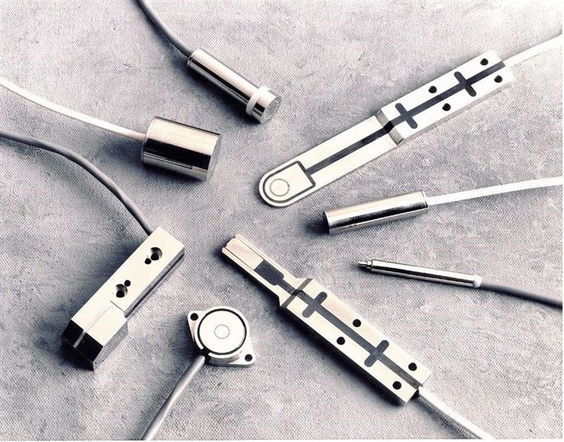
In high-precision manufacturing scenarios such as semiconductor wafer processing, precision machine tool spindle runout detection, and aerospace component deformation monitoring, the accuracy of displacement measurement directly determines product yield and equipment stability.Microsense, as a brand of capacitive displacement sensors, has built a full scene measurement system from sub nanometer to millimeter level, from static positioning to dynamic tracking through passive and active probe technology routes, becoming the "invisible standard" in the field of precision manufacturing.
1、 Passive probe: the cornerstone of linear stability
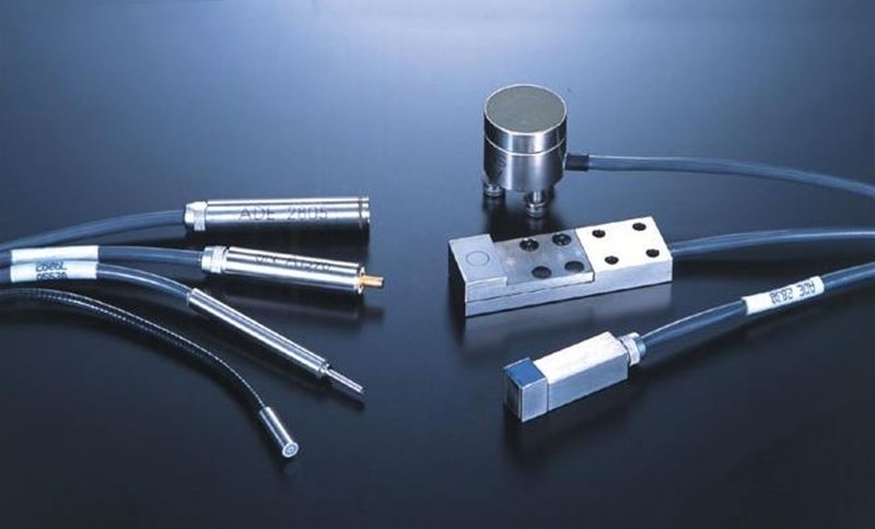
Passive probes, represented by the 48XX, 88XX, and Mini series, use non-contact capacitive induction principle to achieve a dual breakthrough in measurement bandwidth and stability by optimizing probe structure and shielding ring design. Its core advantages lie in:
1. Ultra low linear error:By using Invar alloy probe material and special calibration process, the linearity is controlled within 0.025% of the full range, eliminating periodic errors and hysteresis phenomena.
2. Broadband response capability:Supports bandwidth selection from 1kHz to 20kHz, meeting the dynamic requirements of servo system position feedback, fast tool servo (FTS), and other scenarios.
3. Enhanced environmental adaptability:The ceramic probe housing and IP67 protection level design can withstand temperature changes of -20 ℃ to 85 ℃ and 95% humidity environment, achieving 72 hours of continuous and stable operation in automotive engine thermal deformation monitoring.
2、 Active probe: the "vanguard" of dynamic measurement
To address the measurement challenges of high-speed rotating or oscillating targets, the 58XX and 68XX series active probes integrate driving circuits and intelligent compensation algorithms, breaking through the barrier of nanometer resolution
1. Sub nanometer resolution:The 6810 probe can achieve a displacement resolution of 0.1nm at a bandwidth of 100kHz, and is specifically designed for NRRO (Non Repetitive Runout) detection of hard disk spindle motors and air bearing spindles.
2. Intelligent anti-interference design:By using dynamic shielding loops and adaptive filtering algorithms, electromagnetic interference and the influence of target surface roughness are effectively suppressed. In semiconductor wafer surface inspection, even in the face of nanoscale texture changes, a repeatability accuracy of 0.05nm can still be maintained.
3. Modular expansion capability:Supports flexible configuration of single channel to multiple channels (3U European card rack), and can synchronously collect X/Y/Z three-axis displacement data.
3、 Technology Fusion: A Bridge from Laboratory to Industrialization
The technical value of Microsense probes lies not only in their breakthrough in a single parameter, but also in their deep integration with measurement circuits and software algorithms. For example, its "dynamic calibration technology" can compensate for temperature drift and mechanical vibration in real time, enabling the sensor to maintain long-term stability under complex operating conditions; The open API interface supports seamless integration with platforms such as LabVIEW and MATLAB, accelerating the transformation of scientific research achievements into industrial applications.
From nanoscale semiconductor manufacturing to millimeter scale aerospace component inspection, Microsense capacitive displacement sensor probes redefine the boundaries of precision measurement with a dual engine drive of "passive stability+active precision". With the explosive demand for sub micron precision in intelligent manufacturing, this technological system will continue to empower the localization and replacement of advanced equipment, becoming a key support for China's transition from a "manufacturing power" to a "smart manufacturing powerhouse".