-
E-mail
sales@opton.com.cn
-
Phone
13126536208
-
Address
Oubotong Group, Building 2, No. 1100 Huihe South Street, Chaoyang District, Beijing
Beijing Obotong Optical Technology Co., Ltd
Application of Ultra High Resolution Field Emission Scanning Electron Microscopy in Nanoscience
Date: 2025-12-15Read: 1
Ultra high resolution field emission scanning electron microscopy, as an advanced electron microscopy technique, has been widely applied in the research of nanoscience. Due to its ability to obtain high-resolution images at the nanoscale, it is considered a powerful tool for exploring nanomaterials, nanostructures, and their properties. With the rapid development of nanotechnology, it not only plays an important role in basic research, but also plays a crucial role in the design, manufacturing, and characterization of nanodevices.
Ultra high resolution field emission scanning electron microscopeThe applications in nanoscience are mainly reflected in the following aspects:
1、 Characterization of Nanomaterials
The structure and morphology of nanomaterials are the basis for their unique properties, therefore precise characterization of nanomaterials is crucial. It has extremely high spatial resolution and can observe the surface morphology, particle size, distribution, and other microstructural features of nanomaterials. By using it, the morphology and size distribution of nanostructures such as nanoparticles, nanowires, and nanotubes can be clearly observed, providing important experimental data for the design and performance optimization of nanomaterials.
2、 Morphological analysis of nanostructures
Ultra high resolution field emission scanning electron microscopy can reveal the details of nanostructures with high resolution, especially in the study of nano films, nano coatings, and nano composite materials, showing excellent performance. The surface morphology of nanostructures is an important factor determining their physical and chemical properties, therefore, accurate morphology analysis is crucial for optimizing material performance. In addition, it is widely used to analyze the thickness, uniformity, and adhesion characteristics of nano coatings, which plays an important role in improving the application effect of nano materials in industry.
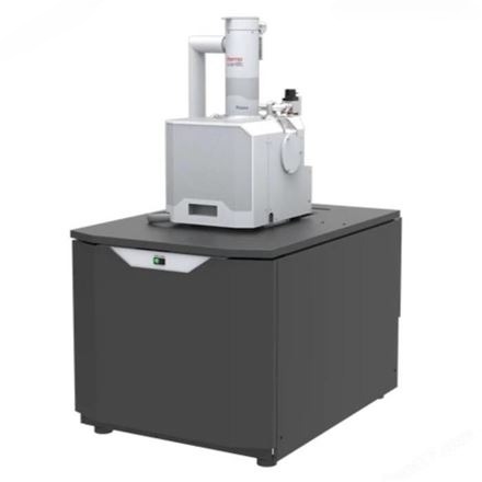
3、 Manufacturing and characterization of nanodevices
With the development of nanotechnology, the application of nanodevices in fields such as semiconductors, electronics, and biosensors is increasing day by day. Plays an important role in the manufacturing and characterization of nanodevices. Its high resolution and excellent 3D imaging capability make it an ideal tool for nanodevice research, especially for monitoring the details of device structures during the preparation process.
4、 Applications in nanobiology
Nanobiology is an important field that combines nanotechnology with biology, and its applications in this field are increasing day by day. Nanomaterials have a wide range of applications in the biomedical field, such as drug delivery systems, cancer treatment, and biosensors. It can also be used to observe the interactions between these nanomaterials and biomolecules and cells, helping researchers gain a deeper understanding of the behavior of nanomaterials in biological systems.
Overall, the application prospects of ultra-high resolution field emission scanning electron microscopy in nanoscience are broad. It can not only provide high-resolution morphology information of nanomaterials, but also provide key support for the manufacturing and characterization of nanodevices, morphology analysis of nanostructures, and applications in nanobiology.