-
E-mail
ahbeq888@163.com
-
Phone
17305697718
-
Address
Beike Feixi Base, No. 6 Yixiu Road, Hefei City, Anhui Province
Anhui Beike Equipment Technology Co., Ltd
PECVD system (plasma enhanced chemical vapor deposition): the core technology for low-temperature and efficient thin film preparation
Date: 2025-11-16Read: 0
The preparation of high-quality thin films is the cornerstone of device performance in fields such as semiconductors, micro nano processing, optical coatings, and new energy materials. The plasma enhanced chemical vapor deposition system, with its plasma enhancement effect, has achieved efficient deposition of high-quality thin films at relatively low temperatures and has become a key process equipment in advanced manufacturing and research and development.
PECVD systemThe core of technology lies in utilizing plasma activity. By exciting the reaction gas (precursor) into a plasma state in a vacuum chamber, a large amount of highly active ions, electrons, and free radicals are generated. These active groups greatly reduce the activation energy required for chemical reactions, thereby bringing two core advantages:
1. Low temperature deposition capability: Compared to traditional thermal CVD, which requires substrate temperatures of hundreds or even thousands of degrees Celsius, PECVD technology typically achieves thin film deposition at temperatures of hundreds or even lower. This characteristic enables it to be widely used in substrates that are not resistant to high temperatures, such as plastic polymers, chips with completed metalized circuits, and flexible electronic substrates, greatly expanding its application scenarios.
2. Excellent film quality and adjustable characteristics: The films prepared by PECVD have the characteristics of density, uniformity, strong adhesion, and good step coverage. By precisely controlling parameters such as plasma power, gas pressure, gas flow rate ratio, and temperature, the stress, refractive index, electrical properties (such as dielectric constant), and stoichiometric ratio of thin films can be effectively regulated to meet diverse application needs.
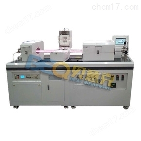
The PECVD system can be used to prepare various functional thin films, including but not limited to:
1. Silicon nitride thin film: As an excellent passivation layer, masking layer, and dielectric layer, it is widely used in integrated circuits and solar cells.
2. Silicon dioxide film: As a commonly used insulating dielectric layer.
3. Amorphous/Microcrystalline Silicon Thin Films: Used for thin-film transistors and thin-film solar cells.
4. Diamond like carbon film: used for wear-resistant and anti friction protective coatings.
The PECVD system successfully combines efficient deposition rate, excellent film quality, and mild process conditions. Its emergence is a major leap forward in thin film preparation technology, providing strong technical support for the development of modern high-tech industries.